


 Dan’s Biz Bookshelf: ‘Abundance: How We Build a Better Future’
 Trouble in Your Tank: In Complex Systems, Design Rules Aren’t Optional
 It’s Only Common Sense: The Phone Is Still Your Competitive Advantage


From Japanese Basket Weaving Art to Nanotechnology with Ion Beams
August 2, 2019 | University of ViennaEstimated reading time: 2 minutes
The properties of high-temperature superconductors can be tailored by the introduction of artificial defects. An international research team around physicist Wolfgang Lang at the University of Vienna has succeeded in producing the world's densest complex nano arrays for anchoring flux quanta, the fluxons. This was achieved by irradiating the superconductor with a helium-ion microscope at the University of Tübingen, a technology that has only recently become available. The researchers were inspired by a traditional Japanese basket weaving art.
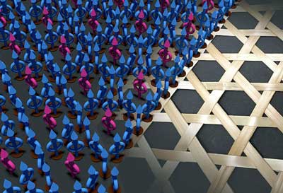
Kagome Inspired Complex Nano Arrays for Anchoring Flux Quanta, the Fluxons
The traditional Japanese basket weaving pattern (kago-mé: basket with eyes) served as an inspiration for an array of fluxon traps produced with a helium-ion microscope in a high-temperature superconductor. The anchored fluxons are represented by blue figures (based on the symbol Φ0 for the flux quantum), the purple fluxons are trapped by their neighbors like in a cage. (Image: Bernd Aichner, University of Vienna)
Superconductors can carry electricity without loss if they are cooled below a certain critical temperature. However, pure superconductors are not suitable for most technical applications, but only after controlled introduction of defects. Mostly, these are randomly distributed, but nowadays the tailored periodic arrangement of such defects becomes more and more important.
Traps and Cages for Magnetic Quantum Objects in Superconductors
A magnetic field can only penetrate in quantized portions into a superconductor, the so-called fluxons. If superconductivity is destroyed in very small regions, the fluxons are anchored at exactly these places. With periodic arrays of such defects, two-dimensional "fluxon crystals" can be generated, which are a model system for many interesting investigations. The defects serve as traps for the fluxons and by varying easily accessible parameters numerous effects can be investigated.
"However, it is necessary to realize very dense defect arrangements so that the fluxons can interact with each other, ideally at distances below 100 nanometers, which is a thousand times smaller than the diameter of a hair," explains Bernd Aichner from the University of Vienna.
Particularly interesting for the researchers are complex periodic arrangements, such as the quasi-kagomé defect pattern investigated in the current study, which was inspired by a traditional Japanese basket weaving art. The bamboo stripes of the kagomé pattern are replaced by a chain of defects with 70 nanometers spacings.
The peculiarity of this artificial nanostructure is that not only one fluxon per defect can be anchored, but approximately circular fluxon chains are formed, which in turn hold a still free fluxon trapped in their midst. Such fluxon cages are based on the mutual repulsion of fluxons and can be opened or locked by changing the external magnetic field. They are therefore regarded as a promising concept for the realization of low-loss and fast superconducting circuits with fluxons.
Nanostructuring of High-Temperature Superconductors with the Helium-Ion Microscope
This research has been made possible by a novel device at the University of Tübingen – the helium-ion microscope. Although it has a similar operating principle as the scanning electron microscope, the helium-ion microscope offers a previously unmatched resolution and depth of field because of the much smaller wavelength of the helium ions.
"With a helium-ion microscope, the superconducting properties can be tailored without removing or destroying the material, which enables us to produce fluxon arrays in high-temperature superconductors with a density that is unrivalled worldwide," emphasizes Dieter Koelle from the Eberhard Karls University of Tübingen.
The scientists are now planning to further develop the method for even smaller structures and to test various theoretically proposed concepts for fluxon circuits.
Share on:


Subscribe
Stay ahead of the technologies shaping the future of electronics with our latest newsletter, Advanced Electronics Packaging Digest. Get expert insights on advanced packaging, materials, and system-level innovation, delivered straight to your inbox.
Subscribe now to stay informed, competitive, and connected.
Suggested Items
AQUANOX A4727 and A4625 Lead KYZEN Offerings at SMTA Oregon Expo and Tech Forum
05/06/2026 | KYZENKYZEN, the global leader in innovative environmentally responsible cleaning chemistries, will exhibit at the SMTA Oregon Expo and Tech Forum scheduled to take place Thursday, May 19 at the Wingspan Event and Conference Center in Hillsboro, Oregon.
Cleaning Is Critical
04/28/2026 | Nolan Johnson, SMT007 MagazineMike Bixenman, president of Magnalytix, and his colleagues Vladimir Sitko, founder of PBT Works, and Adam Klett, PhD, director of science at KYZEN, discussed how cleaning can affect reliability, in a Professional Development Course at APEX EXPO 2026. We spoke to Mike after the session to better understand the context for the current activity in cleaning technology.
KYZEN’s Award-Winning AQUANOX A4618 to Be Featured at SMTA Huntsville and Atlanta Expo & Tech Forums
04/15/2026 | KYZEN'KYZEN, the global leader in innovative environmentally responsible cleaning chemistries, will exhibit at the SMTA Huntsville Expo & Tech Forum, scheduled to take place Tuesday, April 28.
KYZEN Aqueous Chemistries & Process Control Featured at SMTA Arizona Expo & Tech Forum
04/09/2026 | KYZEN'KYZEN, the global leader in innovative environmentally responsible cleaning chemistries, will exhibit at the SMTA Arizona Expo & Tech Forum, scheduled to take place Tuesday, April 21 at the DoubleTree by Hilton in Mesa, AZ.
KOKI Europe Highlights S3X58-HF1200 Solder Paste Benefits
03/30/2026 | KOKI EuropeKOKI Europe, a global leader in advanced soldering materials, is highlighting the capabilities of its S3X58-HF1200 lead-free solder paste, a high-performance SMT material engineered to support today’s demanding electronics manufacturing processes.