


 The Government Circuit: New Council Now Helps Shape Policy Decisions in the Electronics Supply Chain
 Learning With Leo: Soldering—The Interpretation Problem
 Nolan’s Notes: The ROI of Setup Optimization


MIRTEC, ‘The Global Leader in Inspection Technology,’ today announced that it will display its award-winning 3D AOI, 2D AOI and SPI inspection systems in booth #1C55 with Mir Tech-win at the upcoming NEPCON ASIA (NEPCON SOUTH CHINA) exhibition, scheduled to take place August 28-30, 2019 at the Shenzhen Convention & Exhibition Center in China.
MIRTEC’s new partner MTW (Mir Tech-win) will participate in the show. As the name implies, MTW is not just a partner, but another representative of MIRTEC in China.
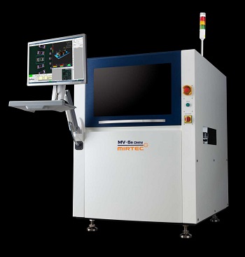
MIRTEC’s award-winning MV-6e OMNI 3D AOI machines are configured with the exclusive OMNI-VISION 3D inspection dystem that combines 15 megapixel CoaXPress camera technology with MIRTEC’s revolutionary Digital Multi-Frequency Quad Moiré 3D system to provide precision inspection of SMT devices on finished PCB assemblies. The proprietary system yields precise height measurement used to detect lifted component and lifted lead defects as well as 3D solder fillet inspection post reflow.
Fully configured, the MV-6e OMNI machine features four (4) 18 megapixel side-view cameras in addition to the 15 megapixel CoaXPress Top-Down camera and an eight (8) phase color lighting system.
The MV-6e In-Line AOI machine is configured with MIRTEC’s 18/10 megapixel inspection technology, which combines an exclusive 8 phase coaxial color lighting system with MIRTEC’s revolutionary Intelli-Scan Laser 3D Inspection system. The MV-6e machine also features four 18 megapixel side-view cameras.
MIRTEC’s exclusive 18 megapixel camera features the highest speed inspection among the 2D AOI system, even though it is configured with 7.3㎛ super precision lens to inspect up to 0201(mm) sized chips. The coaxial light is one of the best inspection solutions for reflective materials such as CSPs (chip scale packages), while its Intelli-Scan 3D Laser scanner provides an ability to find defects on lifted IC leads easily.
MIRTEC’s award-winning MS-11e 3D SPI machine is configured with an exclusive 15 megapixel CoaXPress Camera system, providing enhanced image quality, superior accuracy and incredibly fast inspection rates. The MS-11e uses Dual Projection Shadow Free Moiré Phase Shift imaging technology to inspect solder paste depositions on PCBs post screen print for insufficient solder, excessive solder, shape deformity, shift of deposition and bridging. It uses the same robust platform as MIRTEC’s MV-6 OMNI Series.
“From SPI to 3D AOI, we will show you the best choice of full-coverage in-line inspection systems at NEPCON ASIA,” said Min Kang, president of MIRTEC’s China sales and service division, “The MV-6e will have very high specifications with a low price.”
About MIRTEC
MIRTEC is a leading global supplier of automated inspection systems to the electronics manufacturing industry. For further information, please visit www.mirtec.com.


