


 The Marketing Minute: Marketing With Layers
 The Right Approach: Electro-Tek—A Williams Family Legacy, Part 1
 It’s Only Common Sense: If You’re Not Differentiated, You’re Dead


Flat Lenses With a Twist
August 6, 2019 | KAUSTEstimated reading time: 2 minutes
Ultrathin nanostructured films that control light propagation provide a way of integrating optical components into portable and wearable electronic devices. Twisting a stack of such films offers a simple means to control their behavior and performance, KAUST research shows.
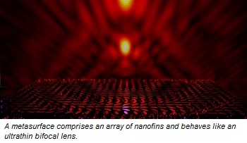
A surface patterned with an array of nanometer-scale structures can change the properties of light passing through it. Each element in the array behaves like a tiny antenna that controls the light’s local phase; that is the relative position of the light wave in its oscillatory cycle. These ultrathin layers are called metalenses because they can focus light just like a conventional, albeit much thicker, glass lens, while being more functional.
“This technology can arbitrarily shape the light pixel by pixel, which is impossible for conventional lenses because of fabrication limitations,” says graduate student Ronghui Lin. “The metalens technology has the potential to replace the huge lens assemblies used in professional reflex cameras with a lens as thin as a postcard.”
One challenge in the development of multifunctional metalenses is their limited efficiency. One possible way to improve this is to stack the metalens. By doing this, Lin and his supervisor, Xiaohang Li, discovered that new phenomenon can be enabled when one metalens is laid on top of another.
The team looked at a metalens with a surface covered in an array of fins or cylinders with an elliptical cross section. By varying the relative orientation of these fins, the lens can add a geometric phase to incoming circularly polarized light. “Consider the rotation of the hands of a clock, which return to the same place every day,” explains Lin. “The rotation angle of these nanofins works in a similar manner. When light passes through these structures, its phase or ‘time’ is changed.” The degree of change depends on the nanofin rotation. This is a powerful tool to manipulate circularly polarized light.
Lin and Li used a mathematical method called finite-difference time-domain simulations to model light propagation in a metalens system comprising two stacked phase elements. Their results showed that by twisting the relative alignment of the two layers, a phenomenon similar to the Moiré effect can be observed (see image below). The team used this phenomenon to develop a bifocal metalens with controllable focal length and intensity ratio. “We believe this multilayer metalens architecture could also apply to other systems and achieve more complicated functionalities,” says Lin.
A Moiré pattern can be formed when two arrays are overlapped and rotated.
Share on:


Testimonial
"Advertising in PCB007 Magazine has been a great way to showcase our bare board testers to the right audience. The I-Connect007 team makes the process smooth and professional. We’re proud to be featured in such a trusted publication."
Klaus Koziol - atgSuggested Items
SMT Perspectives & Prospects: Artificial Intelligence Part 6: Data Module 1
10/07/2025 | Dr. Jennie Hwang -- Column: SMT Perspectives and ProspectsData is one of the six pillars of AI infrastructure. It is critical to the performance of artificial intelligence (AI) models. AI data, essential to both the training and inference of Generative AI models, connotes the datasets used to train, validate, and test AI models. Training data provides models with a frame of reference by establishing a baseline against which models can compare new data using pre-trained models for predictions or generating new content.
U.S. Uses Secret Trackers to Trace AI Chips Diverted to China, Sources Say
08/18/2025 | I-Connect007 Editorial TeamTwo sources told Reuters that U.S. authorities have secretly placed location trackers in some advanced chip shipments they see as at high risk of illegal diversion to China. They said the trackers are intended to locate AI chips that are sent to locations restricted by U.S. export laws, but authorities only examine some shipments.
Happy’s Tech Talk #38: Novel Metallization for UHDI
05/07/2025 | Happy Holden -- Column: Happy’s Tech TalkI have been involved in high-density electronics substrates since 1970 when I joined Hewlett-Packard’s RF semiconductor group after college. Figure 1 shows the difference between trace/space lithography for substrates and silicon starting in 1970. My projects involved sapphire circuits for RF devices, but the figure displays the state of PCBs and integrated CMOS circuits and their packaging, not discreet RF devices. Even then, semiconductors were 50X higher density.
New Database of Materials Accelerates Electronics Innovation
05/05/2025 | ACN NewswireIn a collaboration between Murata Manufacturing Co., Ltd., and the National Institute for Materials Science (NIMS), researchers have built a comprehensive new database of dielectric material properties curated from thousands of scientific papers.
New Database of Materials Accelerates Electronics Innovation
05/02/2025 | ACN NewswireIn a collaboration between Murata Manufacturing Co., Ltd., and the National Institute for Materials Science (NIMS), researchers have built a comprehensive new database of dielectric material properties curated from thousands of scientific papers.