


 Dan’s Biz Bookshelf: ‘Abundance: How We Build a Better Future’
 Trouble in Your Tank: In Complex Systems, Design Rules Aren’t Optional
 It’s Only Common Sense: The Phone Is Still Your Competitive Advantage


Designing a Light-Trapping, Color-Converting Crystal
August 8, 2019 | Stanford UniversityEstimated reading time: 3 minutes
Five years ago, Stanford postdoctoral scholar Momchil Minkov encountered a puzzle that he was impatient to solve. At the heart of his field of nonlinear optics are devices that change light from one color to another - a process important for many technologies within telecommunications, computing and laser-based equipment and science. But Minkov wanted a device that also traps both colors of light, a complex feat that could vastly improve the efficiency of this light-changing process—and he wanted it to be microscopic.
"I was first exposed to this problem by Dario Gerace from the University of Pavia in Italy, while I was doing my PhD in Switzerland. I tried to work on it then but it's very hard," Minkov said. "It has been in the back of my mind ever since. Occasionally, I would mention it to someone in my field and they would say it was near-impossible."
In order to prove the near-impossible was still possible, Minkov and Shanhui Fan, professor of electrical engineering at Stanford, developed guidelines for creating a crystal structure with an unconventional two-part form. The details of their solution were published in Optica ("Doubly resonant χ(2) nonlinear photonic crystal cavity based on a bound state in the continuum"), with Gerace as co-author. Now, the team is beginning to build its theorized structure for experimental testing.
A Recipe for Confining Light
Anyone who's encountered a green laser pointer has seen nonlinear optics in action. Inside that laser pointer, a crystal structure converts laser light from infrared to green. (Green laser light is easier for people to see but components to make green-only lasers are less common.) This research aims to enact a similar wavelength-halving conversion but in a much smaller space, which could lead to a large improvement in energy efficiency due to complex interactions between the light beams.
The team's goal was to force the coexistence of the two laser beams using a photonic crystal cavity, which can focus light in a microscopic volume. However, existing photonic crystal cavities usually only confine one wavelength of light and their structures are highly customized to accommodate that one wavelength.
So instead of making one uniform structure to do it all, these researchers devised a structure that combines two different ways to confine light, one to hold onto the infrared light and another to hold the green, all still contained within one tiny crystal.
"Having different methods for containing each light turned out to be easier than using one mechanism for both frequencies and, in some sense, it's completely different from what people thought they needed to do in order to accomplish this feat," Fan said.
After ironing out the details of their two-part structure, the researchers produced a list of four conditions, which should guide colleagues in building a photonic crystal cavity capable of holding two very different wavelengths of light. Their result reads more like a recipe than a schematic because light-manipulating structures are useful for so many tasks and technologies that designs for them have to be flexible.
"We have a general recipe that says, 'Tell me what your material is and I'll tell you the rules you need to follow to get a photonic crystal cavity that's pretty small and confines light at both frequencies,'" Minkov said.
Computers and Curiosity
If telecommunications channels were a highway, flipping between different wavelengths of light would equal a quick lane change to avoid a slowdown—and one structure that holds multiple channels means a faster flip. Nonlinear optics is also important for quantum computers because calculations in these computers rely on the creation of entangled particles, which can be formed through the opposite process that occurs in the Fan lab crystal—creating twinned red particles of light from one green particle of light.
Envisioning possible applications of their work helps these researchers choose what they'll study. But they are also motivated by their desire for a good challenge and the intricate strangeness of their science.
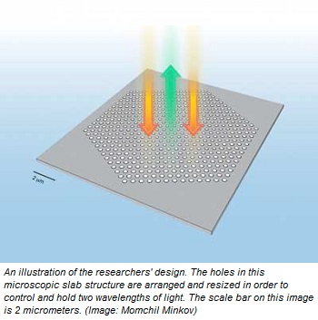
"Basically, we work with a slab structure with holes and by arranging these holes, we can control and hold light," Fan said. "We move and resize these little holes by billionths of a meter and that marks the difference between success and failure. It's very strange and endlessly fascinating."
These researchers will soon be facing off with these intricacies in the lab, as they are beginning to build their photonic crystal cavity for experimental testing.
Share on:


Subscribe
Stay ahead of the technologies shaping the future of electronics with our latest newsletter, Advanced Electronics Packaging Digest. Get expert insights on advanced packaging, materials, and system-level innovation, delivered straight to your inbox.
Subscribe now to stay informed, competitive, and connected.
Suggested Items
Designing Without a Rulebook: When Engineering Becomes Innovation
05/05/2026 | Stephen V. Chavez, Siemens EDAWhat if the very rules that made you successful as a PCB designer are the ones now holding you back? This reminds me of walking the floor and attending sessions at both PCB West 2025 and APEX EXPO 2026, where one common theme stood out: More designs with traditional PCB “best practices” simply don’t apply. It’s not because they’re wrong, but because the problems we’re solving have fundamentally changed. In some cases, those best practices can actually limit performance. This is where PCB design moves beyond optimization and into something far more challenging: designing without a rulebook.
Trouble in Your Tank: In Complex Systems, Design Rules Aren’t Optional
05/06/2026 | Michael Carano -- Column: Trouble in Your TankThere is no question that the electronics industry, especially in circuit board design and fabrication, advanced packaging, and innovation throughout the value chain, has seen a significant transformation, whether it be in materials, system architecture, HDI and ultra HDI, semiconductors, or chiplets. AI and high-performance computing (HPC) are driving change across several fronts, including material properties, assembly techniques (think hybrid bonding), and power management.
Smart Automation: The Journey of a Component Through an SMT Factory
04/22/2026 | Josh Casper -- Column: Smart AutomationIn electronics manufacturing, the SMT line tends to get most of the attention. Placement machines, inspection systems, screen printers, and reflow ovens often take center stage when discussing productivity improvements or new equipment investments. While these systems are obviously critical to the manufacturing process, they only represent a portion of the journey every component takes before becoming part of a finished assembly.
PHOTO GALLERY: Putting in the Work on Standards, Professional Development
04/16/2026 | I-Connect007Behind every standard, innovation, and step forward in electronics are the people who show up to do the work. This week's photo gallery highlights the attendees who filled meeting rooms and classrooms throughout APEX, collaborating on standards development committees, sharing expertise, and investing in their own growth through professional development. These are the faces of progress, gathered not just to learn, but to contribute and shape what comes next.
PHOTO GALLERY: APEX EXPO Receptions Are Where the Industry Comes Together
04/10/2026 | I-Connect007 Editorial TeamAPEX EXPO receptions offer a chance to step away from the booth and connect in a more relaxed setting. From newcomer gatherings to the ice cream social, the show floor reception, and the Golden Gnomes, these events bring attendees together across roles and experience levels. Enjoy this photo gallery of social gatherings. You might find yourself and people you know! It’s a place to reconnect with colleagues, meet people you’ve only known by name, and discover new companies shaping the industry—strengthening relationships and building a sense of community.