


 The Marketing Minute: Marketing With Layers
 The Right Approach: Electro-Tek—A Williams Family Legacy, Part 1
 It’s Only Common Sense: If You’re Not Differentiated, You’re Dead


ULVAC Launches PZT Piezoelectric Thin-film Process Technology and HVM Solution
August 19, 2019 | ACN NewswireEstimated reading time: 4 minutes
ULVAC, Inc. has launched PZT piezoelectric thin-film sputtering technology and a high volume manufacturing (HVM) solution to solve technical issues that have hindered the development of MEMS devices, which are crucial in applications from autonomous driving to next generation wearable terminals (such as smart glasses). The company has begun selling production systems incorporating the new technology.
Evolutions in technologies such as 5G and AI are expected to accelerate the journey towards smart societies, in which the digitization of all types of industries will improve industrial performance and enhance convenience for people. With increasing levels of multi-functionality found in autonomous driving, AR/VR, security, and smartphone applications, actuators are needed in order to activate devices based on signals received from various types of sensors. Demand for actuators is projected to explode and key issues in their development have come to the fore, including the need for miniaturization, reduced production costs, lower power consumption, and higher performance.
It used to be impossible to fabricate PZT piezoelectric thin films, which constitute the key technology in sensors and actuators, using a low-temperature process with the conventional coating method (Sol-Gel). However, in 2015, ULVAC successfully developed the world's most advanced technology for forming PZT piezoelectric thin films using a low-temperature sputtering process. ULVAC has continued developing this as next-generation MEMS technology.
By further advancing this proprietary technology, ULVAC has reduced running costs by optimizing system operation and has greatly improved the technology's reliability, which is critical for device commercialization. The result is a groundbreaking mass-production technology that is now incorporated into systems ULVAC has begun to sell.
This technology allows MEMS devices to be integrated with semiconductors (CMOS), and enables other positive outcomes such as miniaturization, reduced production costs, lower power consumption, and higher performance. It is expected to pave the way for increased use of MEMS devices in sensors and actuators in spatial information sensing and 3D image displays, including smart glasses. The technology will also facilitate MEMS device use in applications such as 3D fingerprint authentication.
ULVAC will continue to spearhead innovations in MEMS device technologies that can be used in a wide range of applications, including etching, sputtering, ashing, and sputtering targets. With all of these contributions, ULVAC plans to remain a driving force in the creation of smart societies.
Overview of the Technology
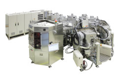
MEMS devices using thin-film PZT are formed on a silicon substrate with the following five (5) layers: an adhesion layer, a lower electrode layer, a buffer layer, a piezoelectric (PZT) layer, and an upper electrode layer. The laminated structure of all these layers can be formed using ULVAC's single-wafer sputtering system without exposing the substrate to the atmosphere. This multi-chamber sputtering system (model SME-200) allows for continuous process flow, optimizing each individual layer inside its own process chamber to achieve high repeatability and improved throughput. The system is also designed to provide a uniform and stable process for forming 8-inch silicon substrates, the largest size substrate available today for MEMS device mass production. A load-lock chamber and a maximum of seven (7) process chambers can be installed, including DC and RF magnetron sputtering chambers, and a rapid thermal annealing (RTA) chamber for accelerating crystallization.
ULVAC's PZT sputtering system uses PZT sputtering chambers specifically designed to solve problems unique to PZT, and it forms PZT thin films by growing crystals on a heated wafer. To do so, ULVAC uses a new low-temperature PZT thin-film process carried out at no more than 500 degrees C, as well as a proprietary process technology for applying a buffer layer, simultaneously achieving superior piezoelectric performance*1 and high reliability*2. Furthermore, through maintenance cycle optimization, running costs have been reduced to 75% of what they were in 2015, resulting in the world's highest PZT thin film performance under mass-production conditions.
Features of the Technology
1. Allows film formation by laminating individual layers inside the same system using a single-wafer sputtering system.
2. Achieves mass production of high-performance PZT thin films using a proprietary low-temperature process technology carried out at no more than 500 degrees C.
3. Achieves high device reliability through the use of a new process.
4. Reduces running costs to 75% of what they were in 2015.
*1 Piezoelectric performance: The higher the piezoelectric constant (e31), the greater the movement per unit of voltage applied to the device, making it possible to miniaturize the device and reduce its power consumption. (Piezoelectric constant e31: -15.5 C/m2 @ PZT film thickness: 2.0 um)
*2 High reliability: As indicators for the device's high level of durability, a dielectric breakdown voltage of around 200 V and a time-dependent dielectric breakdown (TDDB) of 2 million hours were confirmed.
About ULVAC
ULVAC, Inc., founded in 1952, contributes to the development of industry through its comprehensive vacuum technologies. We created ULVAC SOLUTIONS based on these unique technologies and long years of research, development and production innovation. We offer these solutions, for equipment, materials, vacuum components, analytic evaluation and various other services, to manufacturers of electronic components, semiconductors, solar cells, flat panel displays and other industrial equipment. For more information, please visit www.ulvac.co.jp/en/.
Share on:


Testimonial
"The I-Connect007 team is outstanding—kind, responsive, and a true marketing partner. Their design team created fresh, eye-catching ads, and their editorial support polished our content to let our brand shine. Thank you all! "
Sweeney Ng - CEE PCBSuggested Items
Circus SE Set for High-Volume Market Entry in the Defense Sector
10/17/2025 | BUSINESS WIRECircus SE a global technology leader in AI robotics for autonomous nutrition systems and troop supply, is expanding its global production network as part of its high-volume market entry into the defense sector.
China Expands Rare Earth Export Restrictions, Tightening Grip on Global Supply Chains
10/16/2025 | I-Connect007 Editorial TeamChina sharply expanded its rare earth export restrictions on Oct. 9, adding additional elements and refining technologies to its control list while imposing stricter rules on foreign users in the defense and semiconductor industries.
SAMI Advanced Electronics Company Launches “Remal” Computer Manufacturing Project in Partnership with HP and Foxconn
10/15/2025 | SAMI-AECSAMI Advanced Electronics Company (SAMI-AEC), a wholly owned subsidiary of Saudi Arabian Military Industries (SAMI), proudly announced the launch of the “Remal” project for computer manufacturing, in strategic partnership with HP and Foxconn.
The Right Approach: Electro-Tek—A Williams Family Legacy, Part 1
10/15/2025 | Steve Williams -- Column: The Right ApproachThere is no bronze bust in the lobby or portrait in the conference room of Electro-Tek's founder—my Dad, Charles “Chuck” Williams—so with the facility closing last year after 56 years, I feel it is time to tell the story. Chuck Williams founded Electro-Tek in 1968 in our basement, eventually moving into the second floor of an old 1913 building in downtown Milwaukee that is still standing (the first of three eventual facilities).
LPKF Joins productronica’s 50th Anniversary, Showcasing Laser Technology for Electronics Manufacturing
10/10/2025 | LPKF Laser & ElectronicsLPKF Laser & Electronics invites visitors to productronica 2025 in Munich from November 18 to 21. At booth 305 in hall B2, the company will present its portfolio of modern laser technologies for the electronics industry live – from prototyping systems and high-performance depaneling to laser plastic welding for electronic housings and thin glass processing for advanced packaging.