


 Trouble in Your Tank: At 40 GHz, Everything Matters, Part 2
 It’s Only Common Sense: Stop Watching the Headlines and Start Watching the Opportunity
 The Right Approach: The Pros and Cons of PCB Vertical Integration


Scientists from EPFL in Switzerland and Scuola Superiore Sant’Anna in Italy are developing technology for the blind that bypasses the eyeball entirely and sends messages to the brain. They do this by stimulating the optic nerve with a new type of intraneural electrode called OpticSELINE. Successfully tested in rabbits, they report their results in Nature Biomedical Engineering.
“We believe that intraneural stimulation can be a valuable solution for several neuroprosthetic devices for sensory and motor function restoration. The translational potentials of this approach are indeed extremely promising,” explains Silvestro Micera, EPFL’s Bertarelli Foundation Chair in Translational Neuroengineering, and Professor of Bioelectronics at Scuola Superiore Sant’Anna, who continues to innovate in hand prosthetics for amputees using intraneural electrodes.
Blindness affects an estimated 39 million people in the world. Many factors can induce blindness, like genetics, retinal detachment, trauma, stroke in the visual cortex, glaucoma, cataract, inflammation or infection. Some blindness is temporary and can be treated medically. How do you help someone who is permanently blind?
The idea is to produce phosphenes, the sensation of seeing light in the form of white patterns, without seeing light directly. Retinal implants, a prosthetic device for helping the blind, suffer from exclusion criteria. For example, half a million people worldwide are blind due to retinitis pigmentosa, a genetic disorder, but only a few hundred patients qualify for retinal implants for clinical reasons. A brain implant that stimulates the visual cortex directly is another strategy albeit risky. A priori, the new intraneural solution minimizes exclusion criteria since the optic nerve and the pathway to the brain are often intact.
Previous attempts to stimulate the optic nerve in the 1990s provided inconclusive results. EPFL’s Medtronic Chair in Neuroengineering Diego Ghezzi explains, “Back then, they used cuff nerve electrodes. The problem is that these electrodes are rigid and they move around, so the electrical stimulation of the nerve fibers is unstable. The patients had a difficult time interpreting the stimulation, because they kept on seeing something different. Moreover, the cuff electrodes probably had limited selectivity because they recruited superficial fibers.”
Intraneural electrodes may indeed be the answer for providing rich visual information to the subjects. They are also stable and less likely to move around once implanted in a subject, according to the scientists. Cuff electrodes are surgically placed around the nerve, whereas intraneural electrodes pierce through the nerve.
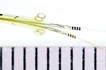
Together, Ghezzi, Micera and their teams engineered the OpticSELINE, an electrode array of 12 electrodes. In order to understand how effective these electrodes are at stimulating the various nerve fibers within the optic nerve, the scientists delivered electric current to the optic nerve via OpticSELINE and measured the brain’s activity in the visual cortex. They developed an elaborate algorithm to decode the cortical signals. They showed that each stimulating electrode induces a specific and unique pattern of cortical activation, suggesting that intraneural stimulation of the optic nerve is selective and informative.
As a preliminary study, the visual perception behind these cortical patterns remains unknown. Ghezzi continues, “For now, we know that intraneural stimulation has the potential to provide informative visual patterns. It will take feedback from patients in future clinical trials in order to fine-tune those patterns. From a purely technological perspective, we could do clinical trials tomorrow.”
With current electrode technology, a human OpticSELINE could consist of up to 48-60 electrodes. This limited number of electrodes is not sufficient to restore sight entirely. But these limited visual signals could be engineered to provide a visual aid for daily living.


