


 The Government Circuit: New Council Now Helps Shape Policy Decisions in the Electronics Supply Chain
 Learning With Leo: Soldering—The Interpretation Problem
 Nolan’s Notes: The ROI of Setup Optimization


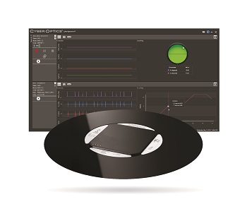
CyberOptics Corporation will exhibit at SEMICON Taiwan, September 18 to 20, 2019 at the Taipei Nangang Exhibition Center in booth # L0310. During the show, the company will launch its new WaferSense auto vibration and leveling sensor (AVLS3) with CyberSpectrum software and the new NanoResolution multi-reflection suppression (MRS) sensor for inspection and metrology in semiconductor applications.
At only 3.5mm, AVLS3 can travel with ease to most fab locations where a wafer travels. The chemically hardened glass (CHG) substrate enables smooth wafer handling and improved vacuum chucking.
With long-range wireless capability, AVLS3 combined with new, easy-to-use CyberSpectrum software, collects and displays both leveling and vibration data simultaneously for fast equipment set-up, alignment and real-time equipment diagnostics.
Additionally, for mid-end and advanced packaging inspection and measurement, CyberOptics will demonstrate the new proprietary NanoResolution MRS sensor technology that meticulously identifies and rejects multiple reflections caused by shiny components and mirror-like surfaces. Effective suppression of multiple reflections is critical for highly accurate measurements.
“There is a dire need in the industry for highly accurate, 100% inspection of semiconductor advanced packaging applications, at a higher speed,” said Dr. Subodh Kulkarni, president and CEO, CyberOptics Corporation, “This is precisely the market we’ve designed the NanoResolution MRS sensor to address, with speeds 2 to 3 times higher than alternate technologies.”
Offering an unparalleled combination of high accuracy, high resolution and speed, MRS sensors are widely used for inspection and measurement in the SMT and semiconductor markets. The new 3-micron NanoResolution (X/Y resolution of 3 micron, Z resolution of 50 nanometer) MRS sensor enables metrology grade accuracy with superior 100% 3D and 2D measurement performance for features as small as 25-micron.
Further, it is two to three times faster than alternate solutions in the marketplace. With data processing speeds in excess of 75 million 3D points per second, the NanoResolution MRS sensor delivers throughput greater than 25 wafers (300mm) per hour. 100% 3D and 2D metrology and inspection can be completed simultaneously at high speed, versus an alternate, slow method that requires two separate scans for 2D and 3D, and only a sampling of a few dies of the 25 wafers.
This best-in-class MRS sensor technology that recently won the Best of the West award at SEMICON West, is ideally suited for the inspection of solder balls and bumps, copper pillars, and other wafer-level and advanced packaging applications where high precision and speed are needed.
About CyberOptics
CyberOptics Corporation (www.cyberoptics.com) is a leading global developer and manufacturer of high-precision 3D sensing technology solutions. CyberOptics’ sensors are used for inspection and metrology in the SMT and semiconductor capital equipment markets to significantly improve yields and productivity. By leveraging its leading edge technologies, the Company has strategically established itself as a global leader in high precision 3D sensors, allowing CyberOptics to further increase its penetration of key vertical markets. Headquartered in Minneapolis, Minnesota, CyberOptics conducts worldwide operations through its facilities in North America, Asia and Europe.
For more information, visit www.cyberoptics.com.


