


 Powering the Future: Why True Ceramic Circuits Are Not Just ‘Better PCBs’
 Global Sourcing Spotlight: The Global Quality Gap—Why Consistency Wins the Contract
 Knocking Down the Bone Pile: Precision Milling of Underfilled SMT Components


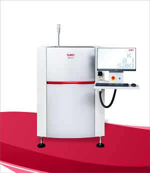
Saki Corporation, an innovator in the field of automated optical and x-ray inspection and measurement equipment, will exhibit its 2Di-LU1 2D bottom-side automated optical inspection (AOI) system at NEPCON Asia along with its 3D AOI and solder paste inspection (SPI) systems and M2M capabilities for ensuring defect-free electronics for automotive and mobile applications. To demonstrate the speed and effectiveness of its 2D bottom-side AOI, Saki is collaborating with Ersa, Wertheim, Germany, to inspect the bottom-side of a printed circuit board assembly (PCBA) after Ersa's SMARTFLOW 2020 selective soldering process.
Saki's 2D line-scan technology is ultra-fast, capturing the image of an entire 460x500mm PCBA and carriers of 610x610mm in one pass, in real time, storing the image into memory, and creating inspection data for the entire board. The system automates the bottom-side inspection process, eliminates board flipping and handling, and ensures quality after the potting, dip, wave, and selective soldering processes.
Both Saki's 3D AOI and SPI systems have a 12 megapixel camera for the fastest inspection and highest resolution on the market. Scalable 7/12/18µm resolution and closed-loop functionality ensure high accuracy and repeatability. The systems are fully compatible and come with the industry's first-of-its-kind Saki Self-Programming (SSP) software. The software eliminates programming, the need for a golden board, and programming errors.
"We are pleased to be able to collaborate with Ersa in presenting selective soldering and 2D bottom-side inspection," said Zheng Ri, general manager of Saki Shanghai Co, Ltd. "As the industry incorporates M2M communication for its high-speed assembly operations, it becomes even more important to join with other equipment manufacturers to ensure that together we have an assembly process that best meets the stringent demands of the market and our customers.
NEPCON Asia (formerly South China), is being held from 28- 30 August 2019, at the Shenzhen Convention and Exhibition Center, Shanghai, China. Saki will be in booth 1G35.
About Saki Corporation
Since its inception in 1994, Saki has led the way in the development of automated recognition through robotic vision technology. Saki's 3D automated solder paste, optical, and x-ray inspection systems (SPI, AOI, AXI) have been recognized to provide the stable platform and advanced data capture mechanisms necessary for true M2M communication, improving production, process efficiency, and product quality. Saki Corporation has headquarters in Tokyo, Japan with offices, sales, and support centers around the world. For more information visit www.sakiglobal.com.


