


 Dan’s Biz Bookshelf: ‘Abundance: How We Build a Better Future’
 Trouble in Your Tank: In Complex Systems, Design Rules Aren’t Optional
 It’s Only Common Sense: The Phone Is Still Your Competitive Advantage


Sticker Makes Nanoscale Light Manipulation Easier to Manufacture
August 26, 2019 | Purdue UniversityEstimated reading time: 2 minutes
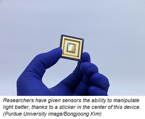
Human pathogens, such as HIV and viruses causing respiratory tract infection, have molecular fingerprints that are difficult to distinguish. To better detect these pathogens, sensors in diagnostic tools need to manipulate light on a nanoscale.
But there isn’t a good way to manufacture these light manipulation devices without damaging the sensors. Purdue University engineers have a solution: Stickers.
In a paper published in Nano Letters, the team integrated light manipulation devices called 3D plasmonic nanoarrays onto peelable films that can stick to any surface. They tested the sticker-nanoarray’s capabilities on the lenses of sensors, which make up conventional imaging systems.
The Air Force Research Laboratory supported the work and validated the sticker’s performance and properties.
“Unlike any existing approaches, the entire process occurs in distilled water at room temperature without the chemical, thermal or mechanical treatments that can damage sensitive surfaces, such as a sensor lens,” said Chi Hwan Lee, an assistant professor of biomedical engineering and mechanical engineering at Purdue.
To turn the nanoarrays into a sticker, the researchers built them into a film on a silicon wafer. When submerged in distilled water, the film peels cleanly from the wafer, allowing the wafer to be reused. The film can then stick to the desired surface without damaging it.
“Because this methodology allows 3D plasmonic nanoarrays to physically separate from a donor wafer and transfer over to another surface without defect, it offers a major cost- and time-saving factor in the manufacturing scheme,” Lee said.
The researchers also demonstrated that the process works for various classes of 3D plasmonic nanoarrays in both lateral and vertical configurations, offering more functionality.
Lee’s lab plans to further develop these sticker-nanoarrays for biological sensing applications, such as for protein detection in clinical diagnostics. The lab has already created electronic stickers that serve as bio-patches for drug delivery. They also can enable ordinary objects to wirelessly connect to a network, creating an “Internet of Things.”
The method has been patented via the Purdue Research Foundation Office of Technology Commercialization. This research aligns with Purdue's Giant Leaps celebration, acknowledging the university’s global advancements made in health, longevity and quality of life as part of Purdue’s 150th anniversary. This is one of the four themes of the yearlong celebration’s Ideas Festival, designed to showcase Purdue as an intellectual center solving real-world issues.
Share on:


Subscribe
Stay ahead of the technologies shaping the future of electronics with our latest newsletter, Advanced Electronics Packaging Digest. Get expert insights on advanced packaging, materials, and system-level innovation, delivered straight to your inbox.
Subscribe now to stay informed, competitive, and connected.
Suggested Items
Connect the Dots: Designing for the Future of Manufacturing Reality—Surface Finish
05/07/2026 | Matt Stevenson -- Column: Connect the DotsWhen designing the complex boards that many electronic devices require to operate, designers should consider manufacturability at every step. This is my last article focused on designing for the always-evolving manufacturing reality. Choosing the right surface finish has always been important. If you are creating intricate designs with a wide variety of components, like for an ultra-high density interconnect (UHDI) board, surface finish is a critical last step.
Elsyca Acquires Hivelix to Strengthen Simulation Platform for Electrochemical Surface Engineering
04/03/2026 | ElsycaElsyca, a global pioneer in computer-aided engineering (CAE) simulation for electrochemical processes and surface finishing, announces the acquisition of Hivelix, a specialist in advanced surface treatment simulation with strong expertise in multiphysics modelling and AI-assisted process optimisation.
Connect the Dots: Designing for the Future of Manufacturing Reality—Solder Mask and Legend
04/09/2026 | Matt Stevenson -- Column: Connect the DotsPCBs seem to be getting more complex by the day, so it is important for designers to keep educating themselves about the realities of manufacturing increasingly intricate boards. Last month’s column highlighted design considerations for the strip-etch-strip process and how manufacturers approach that phase of production. Now that we have a functioning board, we must protect the PCB from environmental hazards and document the circuit components. This article will detail the solder mask and legend process and offer best practices for designers to ensure a high-quality result.
Take the Mic: Photo Chemical Systems: 50 Years Strong
04/03/2026 | Real Time with... APEX EXPOPhoto Chemical Systems is celebrating 50 years in the bare board PCB market. David Graves and Jason Averette discuss how they've expanded into assembly, leveraging strong relationships and a customer-centric approach to navigate supply chain challenges. With innovative solutions and future growth strategies, including AI integration and new market ventures, Photo Chemical Systems continues enduring success.
Bold Laser Automation Introduces Precision Laser Cleaning System for Advanced Manufacturing
03/27/2026 | PRNewswireBold Laser Automation, Inc. has introduced the LPCl1820UV Laser Precision Cleaning System, a Class 1, industrial laser platform engineered for high-precision surface cleaning and thin-film removal in demanding manufacturing environments.