


 Dan’s Biz Bookshelf: ‘Abundance: How We Build a Better Future’
 Trouble in Your Tank: In Complex Systems, Design Rules Aren’t Optional
 It’s Only Common Sense: The Phone Is Still Your Competitive Advantage


Microfluidic Devices Made of Wood
August 28, 2019 | ACSEstimated reading time: 2 minutes
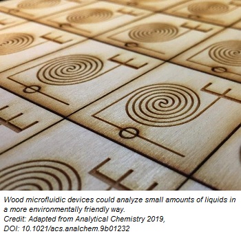
To analyze tiny amounts of liquids, scientists often use devices called microfluidic chips, which are small pieces of plastic that are etched or molded with miniscule channels. Although these single-use chips are small, their widespread use in labs, hospitals and point-of-care situations adds up to a lot of plastic pollution. Therefore, researchers reporting in ACS’ journal Analytical Chemistry have developed versatile microfluidic chips made of a renewable, biodegradable and inexpensive resource—wood.
Microfluidic chips are useful for analyzing small samples, like a single drop of blood, at low cost because only miniscule amounts of expensive reagents are needed. When a fluid flows through the microchannels, it is mixed with certain substances and then analyzed, for example, for the presence of microbes or disease-related proteins. Recently, scientists have tried making microfluidic chips from inexpensive, environmentally friendly resources such as cloth or paper, but these devices are typically limited to relatively simple applications. Govind Rao and colleagues wanted to make a microfluidic device out of low-cost wood that could be used for a variety of purposes.
To make their device, the researchers used a laser printer to engrave tiny channels into birch plywood chips. Then, to prevent liquids from seeping into the porous wood, they coated the channels with a thin layer of Teflon(R). When they introduced blue and red food dyes to the tips of Y- and T-shaped patterns of channels, the liquids mixed as efficiently in the wood chips as in conventional plastic devices. The researchers also used the wood chips, in conjunction with a fluorescence technique, to measure the amounts of two proteins and live bacteria, all of which were similar to the amounts determined by a plastic chip. The wood devices were 10–100 times less expensive than comparable plastic ones and more environmentally friendly. Now, the researchers are working on finding a renewable replacement, such as beeswax or natural oils, for the Teflon coating.
Share on:


Subscribe
Stay ahead of the technologies shaping the future of electronics with our latest newsletter, Advanced Electronics Packaging Digest. Get expert insights on advanced packaging, materials, and system-level innovation, delivered straight to your inbox.
Subscribe now to stay informed, competitive, and connected.
Suggested Items
SMTA Ultra HDI Symposium, Day 1: AI at the Core or Out of the Game
04/13/2026 | Marcy LaRont, I-Connect007It was a beautiful 81°F morning in Arizona last Wednesday as I headed to the third annual SMTA Ultra HDI Symposium, focused on AI and ultra high density interconnect technology. Strategically held as part of Arizona’s Tech Week, this year’s conference took place in Avondale in Phoenix's West Valley. The event moved from the cozy offices of the Peoria Sports Complex (which paid homage to baseball’s spring training world) to the larger Avondale Conference Center, highlighting the importance of this area for electronics manufacturing investment.
PCBAA Sets Its Priorities for 2026: Support in the House and Senate
02/03/2026 | Marcy LaRont, I-Connect007David Schild, executive director of the Printed Circuit Board Association of America (PCBAA), leads an organization focused on the domestic manufacture of PCBs and substrates to support America’s critical microelectronics supply. In the continuation of this interview, David talks about the ways his organization is aligning its priorities with Washington, in particular, the Executive Branch. It might feel like a snail’s pace, but progress could mean financial support and more domestic security, even for the smaller companies.
SMT Perspectives & Prospects: Artificial Intelligence Part 6: Data Module 1
10/07/2025 | Dr. Jennie Hwang -- Column: SMT Perspectives and ProspectsData is one of the six pillars of AI infrastructure. It is critical to the performance of artificial intelligence (AI) models. AI data, essential to both the training and inference of Generative AI models, connotes the datasets used to train, validate, and test AI models. Training data provides models with a frame of reference by establishing a baseline against which models can compare new data using pre-trained models for predictions or generating new content.
U.S. Uses Secret Trackers to Trace AI Chips Diverted to China, Sources Say
08/18/2025 | I-Connect007 Editorial TeamTwo sources told Reuters that U.S. authorities have secretly placed location trackers in some advanced chip shipments they see as at high risk of illegal diversion to China. They said the trackers are intended to locate AI chips that are sent to locations restricted by U.S. export laws, but authorities only examine some shipments.
Happy’s Tech Talk #38: Novel Metallization for UHDI
05/07/2025 | Happy Holden -- Column: Happy’s Tech TalkI have been involved in high-density electronics substrates since 1970 when I joined Hewlett-Packard’s RF semiconductor group after college. Figure 1 shows the difference between trace/space lithography for substrates and silicon starting in 1970. My projects involved sapphire circuits for RF devices, but the figure displays the state of PCBs and integrated CMOS circuits and their packaging, not discreet RF devices. Even then, semiconductors were 50X higher density.