


 Dan’s Biz Bookshelf: ‘Abundance: How We Build a Better Future’
 Trouble in Your Tank: In Complex Systems, Design Rules Aren’t Optional
 It’s Only Common Sense: The Phone Is Still Your Competitive Advantage


Enhancing Materials for Hi-Res Patterning to Advance Microelectronics
August 29, 2019 | Brookhaven National LaboratoryEstimated reading time: 5 minutes
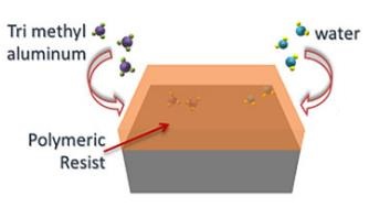
To increase the processing speed and reduce the power consumption of electronic devices, the microelectronics industry continues to push for smaller and smaller feature sizes. Transistors in today’s cell phones are typically 10 nanometers (nm) across—equivalent to about 50 silicon atoms wide—or smaller. Scaling transistors down below these dimensions with higher accuracy requires advanced materials for lithography—the primary technique for printing electrical circuit elements on silicon wafers to manufacture electronic chips. One challenge is developing robust “resists,” or materials that are used as templates for transferring circuit patterns into device-useful substrates such as silicon.
Now, scientists from the Center for Functional Nanomaterials (CFN)—a U.S. Department of Energy (DOE) Office of Science User Facility at Brookhaven National Laboratory—have used the recently developed technique of infiltration synthesis to create resists that combine the organic polymer poly(methyl methacrylate), or PMMA, with inorganic aluminum oxide. Owing to its low cost and high resolution, PMMA is the most widely used resist in electron-beam lithography (EBL), a kind of lithography in which electrons are used to create the pattern template. However, at the resist thicknesses that are necessary to generate the ultrasmall feature sizes, the patterns typically start to degrade when they are etched into silicon, failing to produce the required high aspect ratio (height to width).
As reported in a paper published online on July 8 in the Journal of Materials Chemistry C, these “hybrid” organic-inorganic resists exhibit a high lithographic contrast and enable the patterning of high-resolution silicon nanostructures with a high aspect ratio. By changing the amount of aluminum oxide (or a different inorganic element) infiltrated into PMMA, the scientists can tune these parameters for particular applications. For example, next-generation memory devices such as flash drives will be based on a three-dimensional stacking structure to increase memory density, so an extremely high aspect ratio is desirable; on the other hand, a very high resolution is the most important characteristic for future processor chips.
(Left to right): Ashwanth Subramanian, Ming Lu, Kim Kisslinger, Chang-Yong Nam, and Nikhil Tiwale in the Electron Microscopy Facility at Brookhaven Lab's Center for Functional Nanomaterials. The scientists used scanning electron microscopes to image high-resolution, high-aspect-ratio silicon nanostructures they etched using a "hybrid" organic-inorganic resist.
“Instead of taking an entirely new synthesis route, we used an existing resist, an inexpensive metal oxide, and common equipment found in almost every nanofabrication facility,” said first author Nikhil Tiwale, a postdoctoral research associate in the CFN Electronic Nanomaterials Group.
Though other hybrid resists have been proposed, most of them require high electron doses (intensities), involve complex chemical synthesis methods, or have expensive proprietary compositions. Thus, these resists are not optimal for the high-rate, high-volume manufacture of next-generation electronics.
Page 1 of 3
Share on:


Subscribe
Stay ahead of the technologies shaping the future of electronics with our latest newsletter, Advanced Electronics Packaging Digest. Get expert insights on advanced packaging, materials, and system-level innovation, delivered straight to your inbox.
Subscribe now to stay informed, competitive, and connected.
Suggested Items
SMTA Ultra HDI Symposium, Day 1: AI at the Core or Out of the Game
04/13/2026 | Marcy LaRont, I-Connect007It was a beautiful 81°F morning in Arizona last Wednesday as I headed to the third annual SMTA Ultra HDI Symposium, focused on AI and ultra high density interconnect technology. Strategically held as part of Arizona’s Tech Week, this year’s conference took place in Avondale in Phoenix's West Valley. The event moved from the cozy offices of the Peoria Sports Complex (which paid homage to baseball’s spring training world) to the larger Avondale Conference Center, highlighting the importance of this area for electronics manufacturing investment.
PCBAA Sets Its Priorities for 2026: Support in the House and Senate
02/03/2026 | Marcy LaRont, I-Connect007David Schild, executive director of the Printed Circuit Board Association of America (PCBAA), leads an organization focused on the domestic manufacture of PCBs and substrates to support America’s critical microelectronics supply. In the continuation of this interview, David talks about the ways his organization is aligning its priorities with Washington, in particular, the Executive Branch. It might feel like a snail’s pace, but progress could mean financial support and more domestic security, even for the smaller companies.
SMT Perspectives & Prospects: Artificial Intelligence Part 6: Data Module 1
10/07/2025 | Dr. Jennie Hwang -- Column: SMT Perspectives and ProspectsData is one of the six pillars of AI infrastructure. It is critical to the performance of artificial intelligence (AI) models. AI data, essential to both the training and inference of Generative AI models, connotes the datasets used to train, validate, and test AI models. Training data provides models with a frame of reference by establishing a baseline against which models can compare new data using pre-trained models for predictions or generating new content.
U.S. Uses Secret Trackers to Trace AI Chips Diverted to China, Sources Say
08/18/2025 | I-Connect007 Editorial TeamTwo sources told Reuters that U.S. authorities have secretly placed location trackers in some advanced chip shipments they see as at high risk of illegal diversion to China. They said the trackers are intended to locate AI chips that are sent to locations restricted by U.S. export laws, but authorities only examine some shipments.
Happy’s Tech Talk #38: Novel Metallization for UHDI
05/07/2025 | Happy Holden -- Column: Happy’s Tech TalkI have been involved in high-density electronics substrates since 1970 when I joined Hewlett-Packard’s RF semiconductor group after college. Figure 1 shows the difference between trace/space lithography for substrates and silicon starting in 1970. My projects involved sapphire circuits for RF devices, but the figure displays the state of PCBs and integrated CMOS circuits and their packaging, not discreet RF devices. Even then, semiconductors were 50X higher density.