


 The Right Approach: Get Ready for ISO 9001 Version 6
 Dan’s Biz Bookshelf: ‘Still Broke: Walmart’s Remarkable Transformation'
 Driving Innovation: Depth Routing Processes—Achieving Unparalleled Precision in Complex PCBs


Graphene Sets the Stage for the Next Generation of THz Astronomy Detectors
September 11, 2019 | CHALMERS UNIVERSITY OF TECHNOLOGYEstimated reading time: 2 minutes
Researchers from Chalmers University of Technology have demonstrated a detector made from graphene that could revolutionize the sensors used in next-generation space telescopes.
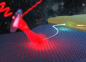
Image Caption: The image depicts a schematic of terahertz (THz) heterodyne detection with graphene. In this, two THz waves (red) are coupled into graphene, where they are combined or mixed. One of the waves is a high intensity signal generated by a local THz light source (i.e. a local oscillator), at a known THz frequency. The other signal is a faint THz wave that mimics the waves coming from space.
Beyond superconductors, there are few materials that can fulfill the requirements needed for making ultra-sensitive and fast terahertz (THz) detectors for astronomy. Chalmers researchers have shown that engineered graphene adds a new material paradigm for THz heterodyne detection.
"Graphene might be the only known material that remains an excellent conductor of electricity/heat even when having, effectively, no electrons. We have reached a near zero-electron scenario in graphene, also called Dirac point, by assembling electron-accepting molecules on its surface. Our results show that graphene is an exceptionally good material for THz heterodyne detection when doped to the Dirac point," says Samuel Lara-Avila, assistant professor at the Quantum Device Physics Laboratory and lead author of the paper.
In detail, the experimental demonstration involves heterodyne detection, in which two signals are combined, or mixed, using graphene. One signal is a high intensity wave at a known THz frequency, generated by a local source (i.e. a local oscillator). The second is a faint THz signal that mimics the waves coming from space. Graphene mixes these signals and then produces an output wave at a much lower gigahertz (GHz) frequency, called the intermediate frequency, that can be analyzed with standard low noise gigahertz electronics. The higher the intermediate frequency can be, the higher bandwidth the detector is said to have, required to accurately identify motions inside the celestial objects.
Sergey Cherednichenko, professor at the Terahertz and Millimetre Wave Laboratory and co-author of the paper, says:
"According to our theoretical model, this graphene THz detector has a potential to reach quantum-limited operation for the important 1-5 THz spectral range. Moreover, the bandwidth can exceed 20 GHz, larger than 5 GHz that the state of the artstate-of-the-art technology has to offer."
Another crucial aspect for the graphene THz detector is the extremely low power needed for the local oscillator to achieve a trustable detection of faint THz signals, few orders of magnitude lower than superconductors require. This could enable quantum-limited THz coherent detector arrays, hence opening the door to 3D imaging of the universe.
Elvire De Beck, astronomer at the Department of Space, Earth and Environment, who did not take part in the research, explains the possible implications for practical astronomy:
"This graphene-based technology has enormous potential for future space missions that aim at e.g. unveiling how water, carbon, oxygen and life itself came to earth. A lightweight, power effective 3D imager that is quantum-limited at terahertz frequencies is crucial for such ambitious tasks. But, at the moment, THz 3D imagers are simply not available".
Sergey Kubatkin, professor at the Quantum Device Physics Laboratory and co-author of the paper, explains:
"The core of the THz detector is the system of graphene and molecular assemblies. This is in itself a novel composite 2D material that deserves deeper investigation from a fundamental point of view, as it displays a whole new regime of charge/heat transport governed by quantum-mechanical effects."
Share on:


Testimonial
"The I-Connect007 team is outstanding—kind, responsive, and a true marketing partner. Their design team created fresh, eye-catching ads, and their editorial support polished our content to let our brand shine. Thank you all! "
Sweeney Ng - CEE PCBSuggested Items
MEMS & Imaging Sensors Summit to Spotlight Sensing Revolution for Europe’s Leadership
09/11/2025 | SEMIIndustry experts will gather November 19-20 at the SEMI MEMS & Imaging Sensors Summit 2025 to explore the latest breakthroughs in AI-driven MEMS and imaging optimization, AR/VR technologies, and advanced sensor solutions for critical defence applications.
Direct Imaging System Market Size to Hit $4.30B by 2032, Driven by Increasing Demand for High-Precision PCB Manufacturing
09/11/2025 | Globe NewswireAccording to the SNS Insider, “The Direct Imaging System Market size was valued at $2.21 Billion in 2024 and is projected to reach $4.30 Billion by 2032, growing at a CAGR of 8.68% during 2025-2032.”
I-Connect007’s Editor’s Choice: Five Must-Reads for the Week
07/04/2025 | Marcy LaRont, I-Connect007For our industry, we have seen several bullish market announcements over the past few weeks, including one this week by IDC on the massive growth in the global server market. We’re also closely watching global trade and nearshoring. One good example of successful nearshoring is Rehm Thermal Systems, which celebrates its 10th anniversary in Mexico and the official opening of its new building in Guadalajara.
Driving Innovation: Direct Imaging vs. Conventional Exposure
07/01/2025 | Simon Khesin -- Column: Driving InnovationMy first camera used Kodak film. I even experimented with developing photos in the bathroom, though I usually dropped the film off at a Kodak center and received the prints two weeks later, only to discover that some images were out of focus or poorly framed. Today, every smartphone contains a high-quality camera capable of producing stunning images instantly.
United Electronics Corporation Advances Manufacturing Capabilities with Schmoll MDI-ST Imaging Equipment
06/24/2025 | United Electronics CorporationUnited Electronics Corporation has successfully installed the advanced Schmoll MDI-ST (XL) imaging equipment at their advanced printed circuit board facility. This significant technology investment represents a continued commitment to delivering superior products and maintaining their position as an industry leader in precision PCB manufacturing.