


 Alpha Insights, Performance by Design: Understanding Heat at the Core of Every Design
 It’s Only Common Sense: Excuses Don’t Pay Invoices
 Trouble in Your Tank: Understanding Interconnect Defects, Part 1


Tunable Optical Chip Paves Way for New Quantum Devices
October 7, 2019 | OSAEstimated reading time: 5 minutes
Researchers have created a silicon carbide (SiC) photonic integrated chip that can be thermally tuned by applying an electric signal. The approach could one day be used to create a large range of reconfigurable devices such as phase-shifters and tunable optical couplers needed for networking applications and quantum information processing.
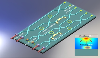
Image Caption: Researchers created the first thermally tunable optical switch using a silicon carbide-on-insulator platform. The schematic image shows their concept for a quantum photonics integrated circuit chip that includes the circular microring resonators and microheaters reported in Optics Letters. The inset shows the temperature and electric field distributions at the cross-section of a microring resonator heated by a microheater. Credit: Ali Adibi, Georgia Institute of Technology
Although most optical and computer chips are made of silicon, there is increasing interest in SiC because it exhibits better thermal, electrical and mechanical properties than silicon while also being biocompatible and operating at wavelengths from the visible to infrared.
In The Optical Society (OSA) journal Optics Letters, researchers led by Ali Adibi from the Georgia Institute of Technology detail how they integrated a microheater and an optical device called a microring resonator onto a SiC chip. The accomplishment represents the first fully integrated and thermally tunable SiC optical switch that operates at near-infrared wavelengths.
“Devices such as the one we demonstrate in this work can be used as building-blocks for next generation quantum information processing devices and to create biocompatible sensors and probes,” said the paper’s first author Xi Wu.
SiC is particularly attractive for quantum computing and communication applications because it has defects that can be optically controlled and manipulated as quantum bits, or qubits. Quantum computing and communication promises to be significantly faster than traditional computing at solving certain problems because data is encoded in qubits that can be in any combination of two states at once, allowing many processes to be performed simultaneously.
Wafer-level manufacturing
The new work builds on the researchers’ previous development of a platform called crystalline SiC-on-insulator that overcomes some of the fragility and other drawbacks of previously reported SiC platforms while providing an easy and reliable route for integration with electronic devices.
“The SiC-on-insulator platform our group pioneered is similar to the silicon-on-insulator technology widely used in semiconductor industry for a variety of applications,” said Tianren Fan, member of the research team. “It enables wafer-level manufacturing of SiC devices, paving the way toward commercialization of integrated photonic quantum information processing solutions based on SiC,” said Ali A. Eftekhar, member of the research team.
Fully exploiting the new platform’s unique capabilities required developing the ability to tune its optical properties so that a single chip-based structure can be used to provide different functions. The researchers accomplished this by using the thermo-optic effect in which changing a material’s temperature modifies its optical properties, such as refractive index.
Caption: The researchers involved in developing the new integrated silicon carbide optical switch include Ali Adibi, Tianren Fan, Xi Wu and Ali A. Eftekhar (left to right). Credit: Ali Adibi, Georgia Institute of Technology
They began by fabricating tiny ring-shaped optical cavities, or microring resonators, using the crystalline SiC-on-insulator technology. In each resonator, light at certain wavelengths, called its resonance wavelengths, traveling around the ring will build up strength through constructive interference. The resonator then can be used to control the amplitude and phase of the light in a waveguide coupled to it. To create a tunable resonator with a high degree of control, the researchers fabricated electric heaters on top of the microrings. When an electric current is applied to the integrated microheater, it locally increases the temperature of the SiC microring and thus changes its resonant wavelengths thanks to the thermo-optic effect.
Page 1 of 2
Share on:


Testimonial
"The I-Connect007 team is outstanding—kind, responsive, and a true marketing partner. Their design team created fresh, eye-catching ads, and their editorial support polished our content to let our brand shine. Thank you all! "
Sweeney Ng - CEE PCBSuggested Items
Real Time with... SMTAI 2025: Innovations in Solder Materials— Kevin Brennan's Journey at Indium
11/05/2025 | Real Time with...SMTAIIn this interview from SMTAI 2025, Kevin Brennan shares his five-year journey at Indium Corporation, where he has worked in R&D, process engineering, and product management. Indium focuses on engineered solder materials, introducing new products like halogen-free and high-temperature alloys to meet industry challenges. The discussion covers a shift to low-temperature alloys to reduce warpage in larger chips and highlights the Indium 12.9 HF flux for high-density boards. Kevin reflects on the supportive community at Indium.
Global Semiconductor Sales Increase 15.8% from Q2 to Q3; MoM Sales Grow 7.0% in September
11/03/2025 | SIAThe Semiconductor Industry Association (SIA) announced global semiconductor sales were $208.4 billion during the third quarter of 2025, an increase of 15.8% compared to Q2.
Strong Demand from CSPs and Sovereign Cloud to Drive Over 20% Growth in AI Server Shipments by 2026
10/30/2025 | TrendForceTrendForce’s latest analysis of the AI server market shows that demand from CSPs and sovereign cloud deployments will remain robust through 2026.
TSMC Fast-Tracks Advanced Chip Technology at Arizona Plant Amid Rising AI Demand
10/27/2025 | I-Connect007 Editorial TeamTSMC said earlier this month that it’s speeding up the rollout of its most advanced chip technology in the US because of rising AI product demand and Intel’s growing competition, The Register reported.
NNME Debuts ChipPath as the Central Gateway for U.S. Semiconductor Careers, Featuring 90,000 Live Job Openings
10/24/2025 | SEMITo help meet the growing demand for skilled workers in the U.S. semiconductor and microelectronics industry, the National Network for Microelectronics Education (NNME), operated by the SEMI Foundation, announced the launch of ChipPath, a first-of-its-kind, AI-enabled career platform that connects individuals directly to real opportunities across the industry.