Decreasing Bend Radius and Improving Reliability—Part I
October 11, 2019 | Kelsey Smith, All FlexEstimated reading time: 1 minute

Application: Design guidelines to improve the flexibility and reliability of flexible circuits.
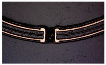
Many of the issues that arise when using a flex circuit come from a lack of knowledge about how to properly design one, especially when the circuit is required to bend. Many novices will design a circuit that calls for bending the flex in too tight of a bend radius, which can cause damage to the circuit and lower the reliability of the end product. This series of articles will focus on the seven key aspects to consider when designing for maximum durability and maximum “flexibility.” It is important to know that because flexibility is a relative term, this study will instead use the phrase "reducing bend radius." Here are two of the seven design strategies (please see Part II and Part III for more tips):
1. Reduce overall thickness:
IPC guidelines typically list minimum bend radius of 6X the circuit thickness for single-sided flex, 10X for double-sided flex, and 20X for multiple layer flex. The area of focus is the thickness where flexing or bending will occur, which should be only in a location with conductors and not plated through-holes. Thickness can best be reduced by:
A. Using thinner copper
B. Using adhesive-less base materials
C. Stagger conductors
D. Specifying button plating or pads only plating
Any flex circuit with plated through-holes will need to be either panel plated or button plated. Button plating is preferred because it only plates the vias and leaves the conductors un-plated and which does not increase the thickness.
2. Use only rolled annealed (RA) copper:
There are two common types of copper; rolled annealed (RA) and electro-deposited (ED) copper.
A. Rolled annealed copper is best for achieving a tighter bend radius.
B. It is also important for you to put on your drawings the direction of the grain in relation to where the tight bending will occur.
Go to Part two of this article.
Testimonial
"We’re proud to call I-Connect007 a trusted partner. Their innovative approach and industry insight made our podcast collaboration a success by connecting us with the right audience and delivering real results."
Julia McCaffrey - NCAB GroupSuggested Items
How Good Design Enables Sustainable PCBs
08/21/2025 | Gerry Partida, Summit InterconnectSustainability has become a key focus for PCB companies seeking to reduce waste, conserve energy, and optimize resources. While many discussions on sustainability center around materials or energy-efficient processes, PCB design is an often overlooked factor that lies at the heart of manufacturing. Good design practices, especially those based on established IPC standards, play a central role in enabling sustainable PCB production. By ensuring designs are manufacturable and reliable, engineers can significantly reduce the environmental impact of their products.
50% Copper Tariffs, 100% Chip Uncertainty, and a Truce
08/19/2025 | Andy Shaughnessy, I-Connect007If you’re like me, tariffs were not on your radar screen until a few months ago, but now political rhetoric has turned to presidential action. Tariffs are front-page news with major developments coming directly from the Oval Office. These are not typical times. President Donald Trump campaigned on tariff reform, and he’s now busy revamping America’s tariff policy.
Global PCB Connections: Understanding the General Fabrication Process—A Designer’s Hidden Advantage
08/14/2025 | Markus Voeltz -- Column: Global PCB ConnectionsDesigners don’t need to become fabricators, but understanding the basics of PCB fabrication can save you time, money, and frustration. The more you understand what’s happening on the shop floor, the better you’ll be able to prevent downstream issues. As you move into more advanced designs like HDI, flex circuits, stacked vias, and embedded components, this foundational knowledge becomes even more critical. Remember: the fabricator is your partner.
MKS’ Atotech to Participate in IPCA Electronics Expo 2025
08/11/2025 | AtotechMKS Inc., a global provider of enabling technologies that transform our world, announced that its strategic brands ESI® (laser systems) and Atotech® (process chemicals, equipment, software, and services) will showcase their latest range of leading manufacturing solutions for printed circuit board (PCB) and package substrate manufacturing at the upcoming 17th IPCA Show to be held at Pragati Maidan, New Delhi from August 21-23, 2025.
MKS Showcases Next-generation PCB Manufacturing Solutions at the Thailand Electronics Circuit Asia 2025
08/06/2025 | MKS Instruments, Inc.MKS Inc, a global provider of enabling technologies that transform our world, today announced its participation in Thailand Electronics Circuit Asia 2025 (THECA 2025), taking place August 20–22 at BITEC in Bangkok.