


 Driving Innovation: Mechanical and Optical Processes During Rigid-flex Production
 It’s Only Common Sense: Your Biggest Competitor Is Complacency
 The Chemical Connection: Onshoring PCB Production—Daunting but Certainly Possible


Stretchable Circuits: New Process Simplifies Production of Functional Prototypes
October 17, 2019 | Saarland UniversityEstimated reading time: 2 minutes
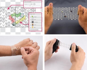
It is based on a so-called laser cutter and its precise, fast cuts. These are provided by easy-to-use software developed by Daniel Gröger and Professor Jürgen Steimle for designers. Since the necessary materials are available on the market, almost any person can now produce stretchable electronics for their own purposes.
A jacket that silences incoming calls when its sleeve is plucked. A bandage that sounds an alarm when the joint is bent too much. These are two of many applications that are only possible with stretchable circuits. "However, current manufacturing processes are time-consuming and very complex," explains Daniel Gröger, a doctoral student in computer science at Saarland University. Hence, together with Professor Jürgen Steimle, Gröger has developed a process to produce stretchable circuits within a few minutes.
The heart of the process is a so-called laser cutter. Its laser beam continuously removes targeted material. In this way, it makes many precise cuts in a very short time. The researchers take advantage of this by having the laser cut a certain pattern into the material, similar to a Y shape. The size of the pattern, the thickness of its lines and the distance between the cuts determine the elasticity of the material. The material consists of a conductive and a non-conductive layer. The circuit is created by the laser ablating the conductive layer at pre-defined points during cutting.
Since it is not only fast, accurate cutting that difficult for humans, but also the planning of where to cut, the researchers have automated that, too. The result is software allowing designers to specify the outline of the piece, similar to a drawing program, and determine which part of it should be stretchable. They determine the degree of elasticity using a virtual slider. Finally, they place the electronic components. The software then calculates the position and nature of the Y shapes, including the circuit diagram, and displays everything. The fast result is unusual, because the calculation of the best ladder route so far has required a lot of computing time and power. The researchers, however, have devised a shortcut by presenting the calculation problem as a graph, for which efficient calculation is possible.
In this way, the researchers produced three prototypes, each taking less than five minutes. The first is a transparent bracelet with a light-emitting diode. On its side is a tab, similar to the rotating wheel on the side of a watch. Pulling on either the strap or on the tab switches the light emitting diode on and off. This fulfills the basic functionality of a stopwatch, says Gröger. Pulling the strap corresponds to starting and stopping. If you pull the wristband, the time measurement starts again. The other two prototypes are a flexible controller for computer games and a sensor that is integrated into an elbow bandage and measures the degree of diffraction.
The materials used, such as plastic foils coated with indium tin oxide, are available online. Gröger therefore believes that the new process also enables people who are not familiar with materials research to create stretchable circuits. The researchers point out that the current test models can withstand at least thousand strains, but this does not yet meet commercial quality criteria for durability. Nevertheless, Gröger is convinced: "Even if the technology still has to be improved, the concepts will hold."
Share on:


Testimonial
"Advertising in PCB007 Magazine has been a great way to showcase our bare board testers to the right audience. The I-Connect007 team makes the process smooth and professional. We’re proud to be featured in such a trusted publication."
Klaus Koziol - atgSuggested Items
Sealed for Survival: Potting Electronics for the Toughest Environments
10/29/2025 | Beth Massey, MacDermid Alpha Electronics SolutionsElectronics deployed in harsh conditions face relentless threats from vibration, impact, chemical contaminants, airborne pollutants, and moisture, conditions that can quickly lead to failure without robust protection. Potting, the process of encapsulating electronics in a protective polymer, is a widely used strategy to safeguard devices from both environmental and mechanical hazards.
Driving Innovation: Mechanical and Optical Processes During Rigid-flex Production
10/28/2025 | Kurt Palmer -- Column: Driving InnovationRigid-flex printed circuit boards are a highly effective solution for placing complex circuitry in tight, three-dimensional spaces. They are now indispensable across a range of industries, from medical devices and aerospace to advanced consumer electronics, helping designers make the most efficient use of available space. However, their unique construction—combining rigid and flexible materials—presents a fundamental challenge for PCB manufacturers.
SMTAI 2025 Review: Reflecting on a Pragmatic and Forward-looking Industry
10/27/2025 | Marcy LaRont, I-Connect007Leaving the show floor on the final afternoon of SMTA International last week in Rosemont, Illinois, it was clear that the show remains a grounded, technically driven event that delivers a solid program, good networking, and an easy space to commune with industry colleagues and meet with customers.
ITW EAE Despatch Ovens Now Support ASTM 5423 Testing
10/15/2025 | ITW EAEAs the demand for high-performance electrical insulation materials continues to grow—driven by the rapid expansion of electric vehicles (EVs) and energy storage systems—thermal processing has become a critical step in material development.
Beyond Thermal Conductivity: Exploring Polymer-based TIM Strategies for High-power-density Electronics
10/13/2025 | Padmanabha Shakthivelu and Nico Bruijnis, MacDermid Alpha Electronics SolutionsAs power density and thermal loads continue to increase, effective thermal management becomes increasingly important. Rapid and efficient heat transfer from power semiconductor chip packages is essential for achieving optimal performance and ensuring long-term reliability of temperature-sensitive components. This is particularly crucial in power systems that support advanced applications such as green energy generation, electric vehicles, aerospace, and defense, along with high-speed computing for data centers and artificial intelligence (AI).