


 Global PCB Connections: Rigid-flex and Flexible PCBs—The Backbone of Modern Electronics
 Flexible Thinking: The Key to a Successful Flex Circuit Design Transfer
 Happy’s Tech Talk #29: Bend-to-Install Semi-flex FR-4


A Technology to Transform 2D Planes Into 3D Soft and Flexible Structures by Engineering Adhesion Between Thin-Films
October 23, 2019 | DGISTEstimated reading time: 2 minutes
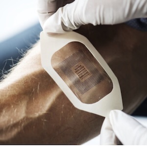
DGIST announced that Professor Sohee Kim’s research team in the Department of Robotics Engineering succeeded in developing a technology to produce flexible 3D medical devices. It is expected to be used in developing various devices with embedded electrical functionality or soft robots.
Professor Sohee Kim’s team developed a new technology for 3D device production that selectively bonds polymeric thin films using plasma. Since this technology can manufacture 3D flexible devices more easily than the existing methods, it is expected to have a positive impact on the future research.
The existing flexible 3D structures could not avoid manual handling such as directly gluing the top and bottom layers of the structure, or transferring pre-strained patterns on the substrate, which has limited the production efficiency at a very low level.
However, Professor Kim’s team created 3D flexible structures by generating covalent bonds only at the edges of patterns formed between two polymeric thin films with plasma and by injecting air into non-bonded patterns (namely, balloons) to inflate them. Moreover, the new 3D structures can be used as a sensor or actuator because metal wires can be easily patterned inside and outside the balloons.
A customized 3D device that is in contact with a complicated surface can also be produced using the technology developed by Professor Kim’s team. Since the 3D device is inflated like a balloon where the device is put on, it can have a customized shape along the curvature of a body part with a complex surface, like the human brain.
In addition, wire patterns in the micrometer scale can be easily formed inside and outside the 3D structure, which has been difficult so far in the production of 3D structures using conventional microelectromechanical systems (MEMS) technologies. It is expected to be widely applied, for instance, for pressure measurement inside the body including the cranium, devices with electrical stimulation and detection functions, and soft robots.
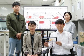
The result of this study was published on the supplementary front page of the ‘ACS Applied Materials & Interfaces’ of the American Chemical Society on Wednesday, October 2. This study was conducted with supports from Basic Research Program of the South Korean Ministry of Science and ICT as well as the DGIST. Ph.D. candidate Hyunmin Moon in the Department of Robotics Engineering and post-doctoral researcher Namsun Chou at Korea Institute of Science and Technology participated in the research as the first co-authors.
Share on:


Testimonial
"The I-Connect007 team is outstanding—kind, responsive, and a true marketing partner. Their design team created fresh, eye-catching ads, and their editorial support polished our content to let our brand shine. Thank you all! "
Sweeney Ng - CEE PCBSuggested Items
Nvidia’s Blackwell Chips Made in Arizona Still Head to Taiwan for Final Assembly
10/27/2025 | I-Connect007 Editorial TeamNvidia has begun production of its next-generation Blackwell GPUs in the United States, but the company still depends heavily on Taiwan to complete the process, The Register reported.
American Standard Circuits Launches 50th 77-Second Webinar
10/27/2025 | American Standard CircuitsAnaya Vardya, President and CEO of American Standard Circuits/ASC Sunstone Circuits is pleased to announce that they have recently unveiled their 50th 77-second webinar.
KYZEN Brings Reliability to Life at productronica 2025 with ANALYST² Process Control Demos
10/22/2025 | KYZEN'KYZEN, the global leader in innovative environmentally responsible cleaning chemistries, will exhibit at productronica 2025, November 18–21 in Munich, Germany, where the company will put a spotlight on its award-winning KYZEN ANALYST² process control system in Hall A4, Stand 450.
SCHMID Group Secures Major Orders for AI Server PCB Production Equipment
10/22/2025 | SCHMID GroupSCHMID Group, a global equipment maker and solution provider for Printed Circuit Boards (PCB) and IC-Substrate manufacturing – announced the successful acquisition of two significant orders in the fast-growing field of PCB for artificial intelligence (AI) server applications. So called AI-Server-Boards.
SEMICON Japan 2025 to Spotlight Sustainability in AI and Semiconductor Innovation
10/22/2025 | SEMISEMICON Japan 2025, the largest gathering of leaders from the microelectronics manufacturing supply chain in Japan, will bring together more than 1,200 exhibitors showcasing semiconductor solutions from December 17-19 at Tokyo Big Sight.