


 Learning with Leo: The Cost of Cleaning and Protecting the Ozone Layer
 Nolan’s Notes: Cleaning With Smaller Geometries
 Standard of Excellence: Building Excellence From the Inside Out


For the first time since multiple acquisitions in recent years, Mycronic AB will demonstrate its full portfolio of electronics assembly solutions at productronica in Munich, November 12-15, 2019. In addition to the latest integrated SMT line, jet printing, dispensing, 3D inspection and material handling solutions, the company will highlight its industry-leading automotive camera module assembly and high-precision die bonding solutions.
Enhancing quality, flexibility and productivity
As electronics assembly continues to grow more complex, Mycronic will be showcasing more ways than ever before to improve quality, flexibility and productivity in a range of electronics manufacturing applications. PCB manufacturers will experience new advances in machine-to-machine communication, full SMT line capabilities and automated material handling systems. Automotive electronics manufacturers will gain expertise in the industry-leading Camera Module Assembly and Test (CMAT) system. And manufacturers of advanced photonic and radio-frequency devices will learn more about the industry's first 1.5 micron die bonder for high-precision, high-volume manufacturing.
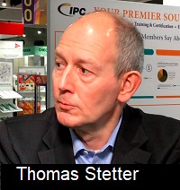
"All of these state-of-the-art solutions are part of our vision to enable zero-defect assembly with the highest utilization for any product mix," says Thomas Stetter, Sr. VP, Assembly Solutions. "From integrated SMT production lines to advanced packaging and automotive sensors, our aim is to enhance our customers' control over the data, processes and material flows that matter most to their success."
New production insights with enhanced M2M communication
As an active member of the Hermes Standard Initiative, the majority of Mycronic's machine models will now be Hermes compliant. This standardized machine-to-machine communication protocol represents an important step in enabling customers to look beyond discrete manufacturing process steps and gain holistic insights into factory-wide productivity. It will also allow greater vendor-independent capabilities, enabling customer processes and programming to become increasingly driven by board requirements.
Full SMT line solution with expanded capabilities
The recently launched MYPro Line, the company's latest full SMT line solution, will demonstrate a number of new software and automation capabilities at productronica. The SIGMA Link software, which correlates data between solder paste inspection and automated optical inspection, now features more intuitive process controls to further improve inspection efficiency and first pass yield. A new AOI platform with 2x faster programming. A new solder paste inspection and jet printing repair system closes several data feedback loops to automatically increase yield and product quality over time. And a new dashboard and analysis software will demonstrate new ways to simplify production scheduling and enhance overall equipment effectiveness.
New advances in conformal coating and plasma treatment
As part of Mycronic's rapidly evolving MYSmart series of dispensing and conformal coating robots, a number of new hardware and software innovations will be on display at productronica 2019. The industry-leading MYC50 conformal coating system, with its new intuitive user interface, precision spray valve and flow monitoring system, promises to deliver even higher levels of precision, repeatability and yield. In addition, a new series of MYS plasma systems will be launched. The MYS systems offer all the benefits of traditional vacuum plasma systems at atmospheric pressure, with safer, cleaner operations and up to 50 times faster cleaning speeds.
Collaborative robotics for autonomous material handling
In a significant step towards improving labor utilization, Mycronic will also demonstrate a next-generation collaborative robotics system. The solution, developed in collaboration with industry-leading partners, will show the potential for entirely operator-independent retrieval, kitting and distribution of component reels.
High-performance automotive camera module assembly
In addition to these new SMT capabilities, Mycronic will also present the manufacturing solutions and experts behind the industry-leading CMAT system. The millions of sensor modules assembled every year by manufacturers using this system are enabling enhanced automotive safety and, ultimately, autonomous driving. Mycronic's process experts will answer questions regarding design for manufacturing, rapid prototyping, application enhancement and full-scale manufacturing optimization.
Advanced die bonding systems
Finally, visitors to productronica will have the opportunity to learn about the industry's leading high-precision die bonding systems for flexible high-speed assembly of optoelectronics and microelectronics. Mycronic's die bonding experts will be on hand to discuss their complete, cost-effective assembly solutions for all levels of advanced packaging.
To experience live demos and to learn more about Mycronic's MYPro Line, CMAT, die bonding and other assembly solutions, visit Booth A3 341 at productronica in Munich, November 12-15, 2019.
Contact at Mycronic: mycronic.com.


