


 Learning with Leo: The Cost of Cleaning and Protecting the Ozone Layer
 Nolan’s Notes: Cleaning With Smaller Geometries
 Standard of Excellence: Building Excellence From the Inside Out


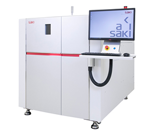
Saki Corporation, an innovator in the field of automated optical and X-ray inspection and measurement equipment, introduces a compact, lightweight, inline 3D-CT automated X-ray inspection machine, the 3Xi-M110, for inspection of printed circuit board assemblies (PCBAs). The 3Xi-M110 reduces the dose and exposure to X-rays during inspection and features new soldering quality inspection functions for PCB assembly applications. Saki will demonstrate the PCB inspection capabilities of the 3Xi-M110 at productronica 2019, being held in Munich, Germany from November 12-15, in stand A2.259.
Saki's new X-ray inspection system ensures the quality of hidden solder joints for bottom-electrode packages, such as BGAs, LGAs, and QFNs, which are found in advanced embedded devices, telecommunications, and automotive products. Saki's Planar Computed Tomography (PCT) provides precise volumetric measurements and shape reconstruction to find voids, head-in-pillow (HiP), and other defects that are extremely difficult to identify.
The 3Xi-M110 hardware platform is 1,380mm wide and weighs 3,100kg, making it 40% lighter and reducing its footprint by 25% over its predecessor. Manufacturing floorspace is saved, it's easy to install, and production-line operation is significantly improved. Although the cast iron frame is lighter in weight, it maintains the rigidity needed for stable operation and accuracy, while the imaging range has been optimized to handle board sizes up to 360 x 330mm (W x L). For larger 360 x 510mm (W x L) boards, 2-step image capture is available.
The 3Xi-M110 delivers exceptional speed and accuracy by utilizing a double motor-driven system equipped with a high-precision linear scale manufactured by Magnescale Co., Ltd. to optimize power and precision. Saki's enhanced PCT technology algorithm improves image capture speed by 30%, reducing production-line takt time.
One of the most significant features of the new system is Saki's revolutionary X-ray tube, which can reduce X-ray exposure up to 70% by powering on the X-rays only at the moment of image capture. An exposure dose simulator allows the user to monitor the radiation dose. Based on that information, the method and magnification for releasing the X-rays can be set. The new X-ray tube design does not require periodic maintenance or spare parts, and the built-in monitoring system reports when the tube needs replacing.
"In the automotive and communications industries, where quality assurance is important, the effectiveness of high-precision, high-quality PCB X-ray inspection has become critical," said Masahide Iino, director and head of the sales division of Saki Corporation. "Saki will continue to respond to the needs of the market by leveraging the accumulated knowledge and experience it has gained through its history as a leading innovator in the field of 2D/3D automated optical inspection and X-ray inspection."
For more information on the 3Xi-M110, please contact Saki at pr@sakicorp.com, or visit our website at www.sakicorp.com or www.sakiglobal.com.


