


 The Marketing Minute: If Your Marketing Budget Gets Cut in Half, Then What?
 Punching Out: How Are the Big Boys in Electronics Doing?
 It’s Only Common Sense: Complexity Is the Enemy of Profit


ALTIX Introduces New ‘ADIX SA neo’ Direct Imager
November 18, 2019 | ALTIXEstimated reading time: 2 minutes
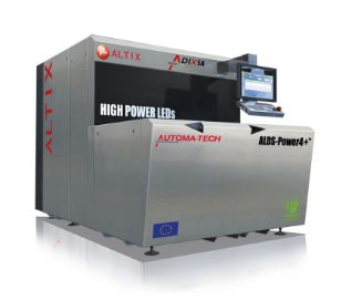
ALTIX, a worldwide leader in UV imaging systems, is proud to introduce its all new Direct Imaging ADIX SA neo, which they presented last week at productronica 2020 in Munich.
ADIX SA neo is an all new panel direct imaging exposure system, dedicated to all resists including dry film and soldermask.
Compared to ADIX SA, the ADIX SA neo provides a 20 to 30% higher productivity. The new model features a linear motor-driven Z-axis and HD DMD coupled to an enlarged optics providing a higher UV light output.
These enhanced unique features bring a wider UV projection width (45mm instead of 20mm) to reduce the number of printed stripes and provide a larger depth of focus. In addition, ADIX SA neo can be customized to match with customers' productivity and budget, from 1 to 7 photo heads and 2 to 3 printed stripes per photo head (equipped with 4 UV wavelength LEDs per head).
Both ADIX SA and ADIX SA neo can be equipped with automated solutions. ADIX CS/F is our compact standard/flip island of automation and ADIX PT/F is our pass-through/flip in-line automation.
Altix also exhibited their fully automatic roll-to-roll direct imaging, the ADIX RtR, at productronica. This equipment combines 30 years of ALTIX know-how of roll-to-roll contact printers in association with the latest direct imaging technologies. Digital printing of flexible circuitry in web is now available.
In addition to the direct imaging product line, ALTIX is offering a wide range of contact printers using innovative LedLight™ sources. ALTIX is active in contact UV exposure solutions by innovating and adapting solutions to new customers’ requirement.
About ALTIX
Founded in 1991, ALTIX is a worldwide specialist in UV imaging systems, operating at the leading edge of technology, providing photolithography solutions mainly for printed circuit board (PCB), flexible printed circuit board (FPC) and photochemical milling (PCM) industries. Headquartered in Normandy, France, this ALTIX location includes R&D center, manufacturing, sales & marketing departments.
Innovation after innovation, ALTIX has delivered hundreds of machines and more than 600 units are currently producing every day, all over the world. Definitively, ALTIX is recognized as a world leader for contact imaging systems and versatile Direct Imaging.
Share on:


Testimonial
"We’re proud to call I-Connect007 a trusted partner. Their innovative approach and industry insight made our podcast collaboration a success by connecting us with the right audience and delivering real results."
Julia McCaffrey - NCAB GroupSuggested Items
Gregoire Outters Promoted to President of Teledyne Marine Group
04/06/2026 | TeledyneTeledyne Technologies Incorporated announced the promotion of Gregoire Outters to President of its Teledyne Marine Group.
Teledyne Strengthens Commitment to the Space Sector
04/01/2026 | BUSINESS WIRETeledyne Technologies Incorporated is excited to announce the integration of the company’s extensive portfolio of space-focused technologies and businesses, reinforcing its long-term commitment to the global space sector.
Teledyne to Supply Detectors for Lazuli Space Observatory
03/30/2026 | BUSINESS WIRETeledyne Space Imaging, part of Teledyne Technologies Incorporated has been awarded a contract by Schmidt Sciences to deliver advanced near-infrared (NIR) H4RG-10 flight focal plane arrays (FPAs) and custom electronics for integration into the Integral Field Spectrograph on the groundbreaking Lazuli Space Observatory.
New Superconducting Chip Could Enable Breakthrough Nondestructive Terahertz Imaging
03/23/2026 | University of GlasgowA tiny crystal chip which uses terahertz radiation to see clearly through a wide range of materials could find applications in healthcare, biological research, and security screening.
The Test Connection Adds Creative Electron Prime TruVision™ X-ray and CT System for Deeper Failure Analysis
03/05/2026 | TTCIThe Test Connection Inc. (TTCI), a trusted provider of electronic test and manufacturing solutions for more than 45 years, has added the Prime TruVision™ X-ray and computed tomography (CT) inspection system from Creative Electron to its engineering and analysis services.