


 The Hidden Enabler of Autonomous Warfare: Advanced PCB Technologies Behind Defense AI
 It’s Only Common Sense: Stay Curious, My Friends


The school participated in the recent Massachusetts STEM Week Challenge 2019 as part a of the statewide effort to boost the interest, awareness and ability for all learners to envision themselves in STEM education and employment opportunities.
The theme for the second annual statewide STEM Week was “See Yourself in STEM.”
“We need more young people to see themselves in STEM careers, and the week’s activities gave students terrific experience in these fields,” Superintendent Joseph Mastrocola said. “It was great to see so much hands-on learning, as well as students taking part in special projects that will benefit the entire school community and residents of Lowell.”
Instructors participating in STEM Week included Lorrie Campbell, the coordinator of STEM outreach and academic success; history teachers Jennifer Parkhurst and Karen Washington; science teachers Kelly Griffin and Nate Howe; and math teachers Judy Moran, Stacey O’Keefe, Devin McInerney, Helen Sullivan and Andrea Collins.
In history class, students considered how integrated electronics have become in peoples’ lives, how dependent people have become on technology and how electronics help us. They defined what an electronic is, and described the typical components of common electronic devices.
Science students participated in a two-day laboratory experiment, setting up a simulation of the copper etching process for creating circuit boards found in many electronic components. They were shown that this manufacturing process creates e-waste that requires proper disposal. The students considered the pros and cons of various disposal methods for the virtual water created in their circuit-board simulation.
In math classes, students defined e-waste and discussed the high volume of the e-waste problem. They identified familiar examples of common products designed with planned obsolescence versus those designed to last. Students evaluated trade-offs associated with the usage of electronics.
Several special projects were also undertaken by students during the week, including Information Technology students in Paul McNeil and Steven King’s classes. Students were chosen to present the projects to school administrators and other staff members who visited classrooms to observe STEM Week activities.
McNeil’s students installed a KVM (keyboard, video and mouse) switch and additional cables to the new Windows computers and a new Apple Mac mini-computer. The switch allows students to use a single workstation to control multiple computers with the touch of a button. Students can use the workstation to learn about building iPhone and Apple apps. The curriculum is used to prepare the students for the AP Computer Science exam and the App Development with Swift Certification Level 1.
The presenter for the project was Information Technology sophomore Abbey Gingras of Dracut.
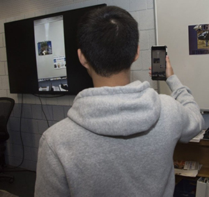
King’s students worked on a GLTech AR app, which uses Augmented Reality to display a video representing Greater Lowell Tech programs on posters that can be hung anywhere in the school. To use the app, students point their iPhone at one of the technical program posters and the poster turns into a video for the appropriate shop.
Design & Visual Communications students created the posters. The app is currently in the Apple beta testing and review process, and the school hopes to have it available soon for all to download from the App Store.
Presenters for the project included Information Technology senior Andrew Seak of Lowell.
Engineering teacher Susan Youens has also been working with her students, including Engineering senior Shayla Som of Lowell on the design of a multifunction building to support youth sports at Shedd Park in South Lowell.
The building will serve as Shayla’s Term 1 project. She is serving as the main drafter/designer of the plans for the building, which is expected be open for the summer and spring sports seasons.
The project is based on a community service idea to create a new concession stand with bathrooms for the park, which Shayla said she chose as a way to gain real-world experience in architectural and civil engineering.
When STEM Week activities were concluded, students participated in a real-world problem to solve in the form of a cellphone recycling program, allowing them to receive hands-on experience with reducing e-waste. Boxes within the school were set up to collect old cellphones, preventing them from ending up in a landfill.


