-

- News
- Books
Featured Books
- smt007 Magazine
Latest Issues
Current Issue
What's Your Sweet Spot?
Are you in a niche that’s growing or shrinking? Is it time to reassess and refocus? We spotlight companies thriving by redefining or reinforcing their niche. What are their insights?

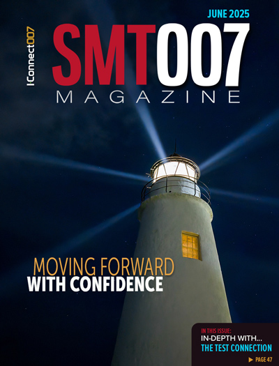
Moving Forward With Confidence
In this issue, we focus on sales and quoting, workforce training, new IPC leadership in the U.S. and Canada, the effects of tariffs, CFX standards, and much more—all designed to provide perspective as you move through the cloud bank of today's shifting economic market.

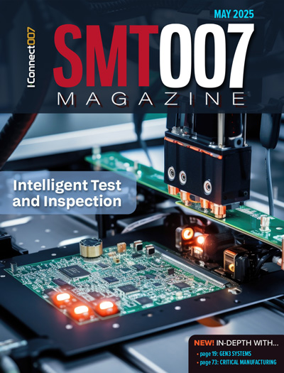
Intelligent Test and Inspection
Are you ready to explore the cutting-edge advancements shaping the electronics manufacturing industry? The May 2025 issue of SMT007 Magazine is packed with insights, innovations, and expert perspectives that you won’t want to miss.
- Articles
- Columns
- Links
- Media kit
||| MENU - smt007 Magazine
iNEMI Call for Participation Webinar Dec. 12
December 6, 2019 | iNEMIEstimated reading time: 1 minute
Flip chip electronic packages are commonly used to address today’s high-density interconnect needs. However, the formation of small voids (microvoids) can occur in solder-based flip chip joints during the assembly process and these voids tend to grow after multiple reflows. This can be a concern for certain applications that involve high electrical and thermal flux across the flip chip where void formation can have an impact on electromigration in the joint. The presence of a void can accelerate complete open failure due to electromigration.
This project will study voids in flip chip interconnect to determine their location and volume. It will also seek to understand how voiding in 1st level interconnect affects product reliability and what level of voiding is acceptable while maintaining reliability requirements. The project will have two distinct phases:
- Phase 1: Determine recommended inspection capabilities for micro-voids in 1st level interconnect materials
- Phase 2: Determine the relationship between voids and the electrical and mechanical reliability of the assembly
The project is expected to develop technical guidelines regarding acceptable voiding characteristics for flip chip interconnects that can be shared with industry and relevant standards bodies.
The 1st Level Interconnect Void Characterization Project is led by Lee Kor Oon (Intel) as project leader, with Sze Pei Lim (Indium) and Kiyoshi Ooi (Shinko) as co-leaders. Click here for additional project information.
Call-for-Participation Webinars
If you are interested in this project, please join us for one of our call-for-participation webinars. These webinars are open to industry (iNEMI membership is not required). Participants must register in advance. Click on the links below to register. For additional information, please contact Masahiro Tsuriya (m.tsuriya@inemi.org).
Session 1 (APAC)
Date: December 12, 2019
Time: 10:00 a.m. JST (Japan)
9:00 a.m. CST (China)
8:00 p.m. EST (U.S.) on Dec. 11
5:00 p.m. PST (U.S.) on Dec. 11
Session 2 (Americas and EMEA)
Date: December 12, 2019
Time: 7:00 a.m. EST (U.S.)
1:00 p.m. CET (Europe)
8:00 p.m. CST (China)
9:00 p.m. JST (Japan)
Suggested Items
Hands-On Demos Now Available for Apollo Seiko’s EF and AF Selective Soldering Lines
06/30/2025 | Apollo SeikoApollo Seiko, a leading innovator in soldering technology, is excited to spotlight its expanded lineup of EF and AF Series Selective Soldering Systems, now available for live demonstrations in its newly dedicated demo room.
Indium Corporation Expert to Present on Automotive and Industrial Solder Bonding Solutions at Global Electronics Association Workshop
06/26/2025 | IndiumIndium Corporation Principal Engineer, Advanced Materials, Andy Mackie, Ph.D., MSc, will deliver a technical presentation on innovative solder bonding solutions for automotive and industrial applications at the Global Electronics A
Fresh PCB Concepts: Assembly Challenges with Micro Components and Standard Solder Mask Practices
06/26/2025 | Team NCAB -- Column: Fresh PCB ConceptsMicro components have redefined what is possible in PCB design. With package sizes like 01005 and 0201 becoming more common in high-density layouts, designers are now expected to pack more performance into smaller spaces than ever before. While these advancements support miniaturization and functionality, they introduce new assembly challenges, particularly with traditional solder mask and legend application processes.
Knocking Down the Bone Pile: Tin Whisker Mitigation in Aerospace Applications, Part 3
06/25/2025 | Nash Bell -- Column: Knocking Down the Bone PileTin whiskers are slender, hair-like metallic growths that can develop on the surface of tin-plated electronic components. Typically measuring a few micrometers in diameter and growing several millimeters in length, they form through an electrochemical process influenced by environmental factors such as temperature variations, mechanical or compressive stress, and the aging of solder alloys.
SolderKing’s Successful Approach to Modern Soldering Needs
06/18/2025 | Nolan Johnson, I-Connect007Chris Ward, co-founder of the family-owned SolderKing, discusses his company's rapid growth and recent recognition with the King’s Award for Enterprise. Chris shares how SolderKing has achieved these award-winning levels of service in such a short timeframe. Their secret? Being flexible in a changing market, technical prowess, and strong customer support.


