


 The Marketing Minute: If Your Marketing Budget Gets Cut in Half, Then What?
 Punching Out: How Are the Big Boys in Electronics Doing?
 It’s Only Common Sense: Complexity Is the Enemy of Profit


PV Nano Cell Successfully Prints Inside VIA for High-Demanding Application
February 6, 2020 | PV Nano CellEstimated reading time: 2 minutes
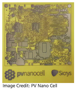
PV Nano Cell, Ltd. (OTC: PVNNF) ("PV Nano Cell" or the "Company"), an innovative provider of inkjet-based conductive digital printing solutions and producer of conductive digital inks, today announced that it has successfully printed and tested high-demanding parts that include printing inside challenging VIA—vertical interconnect access.
VIA are used as an electrical connection between layers (or sides of substrate) in a physical electronic circuit that goes through the plane of one or more adjacent layers. PV Nano Cell was able to print inside VIA with a diameter of 0.6 mm (0.024 inch) and a height of 1 mm (0.04 inch). A phenomenal, minimal resistance of 0.1 ohms was measured and the company said it could print smaller sized VIA as well. One side of the substrate is printed a pattern consisting of multiple widths and thicknesses (heights) of conductive features. This pattern forms an accurate resistor that heats to high temperature in less than milliseconds.
PV Nano Cell’s Chief Executive Officer, Dr. Fernando de la Vega, commented, “In this special application, we first print inside the VIA. Then we print the first designated pattern on one side of the FR-4 (glass-reinforced epoxy laminate material). The substrate is then flipped over and we print the second designated pattern on the other side of the FR-4. The VIA printed in the beginning of the process electrically connects between the two patterns printed on the two sides of the FR-4 substrate. The unique printing process that we developed cuts approximately 50% of the cost of production compared to the existing manufacturing solution. We are positive we can improve the process even more and print smaller-sized VIA.”
PV Nano Cell is implementing these technologies and products to provide a complete solution approach that allows customers to fully realize the potential of inkjet based electronics printing for mass production applications. The company’s proven solution includes its proprietary Sicrys™, silver-based conductive inks, inkjet production printers and the complete printing process.
PV Nano Cell’s Chief of Business Development Officer, Mr. Hanan Markovich commented, "The printed parts have gone through intensive, high-demanding standard testing by the customer and we expect the production to begin in the near future. Such an achievement demonstrates again, the feasibility and attractiveness of PV Nano Cell’s solutions for mass production applications.“
PV Nano Cell, Ltd.
PV Nano Cell (PVN) offers the first-ever complete solution for mass-produced inkjet based, printed electronics. The proven solution includes PVN’s proprietary Sicrys™, silver-based conductive inks, inkjet production printers and the complete printing process. The process includes ink properties' optimization, printer’s parameters setup, printing modifications & tailored printing instructions per application. In the heart of PVN’s value proposition lies its unique and patented conductive silver and coper inks - Sicrys™. Those are the only inks made of Single Nano Crystals – which allows the inks to have the highest stability and throughput required to drive optimal mass-production results for wide range of applications. PVN’s solutions are used all over the world in a range of digital printing applications including: automotive, photovoltaics, printed circuit boards, flexible printed circuits, antennas, sensors, heaters, touchscreens and other. For more information, please visit http://www.pvnanocell.com/
Share on:


Testimonial
"In a year when every marketing dollar mattered, I chose to keep I-Connect007 in our 2025 plan. Their commitment to high-quality, insightful content aligns with Koh Young’s values and helps readers navigate a changing industry. "
Brent Fischthal - Koh YoungSuggested Items
Ventec Evaluates US Manufacturing Facility to Support North American Growth
04/28/2026 | Ventec International GroupVentec International Group today announced that it is evaluating the potential establishment of a manufacturing facility in the United States to support its growing North American customer base with high-performance laminate and prepreg materials.
Roundtable: Advanced Materials
04/27/2026 | I-Connect007 Editorial TeamDriven largely by the need for advanced chip technology for super compute ability and AI applications, low Dk, low-loss resin systems, and heavy copper laminate are attracting significant attention and global resources. There are numerous unavoidable challenges in this market that will impact manufacturers and the supply chain, and they may be hitting critical mass sooner than OEMs and fabricators think. In this roundtable discussion, moderator Marcy LaRont speaks with topic experts: Mark Goodwin, John Fix, and Ed Kelley.
Fresh PCB Concepts: Designing PCBs for Harsh Environments—Reliability Is Engineered Upstream
04/23/2026 | Team NCAB -- Column: Fresh PCB ConceptsWhen engineers hear the phrase “harsh environment,” they usually think of the extreme temperature swings, vibration and shock, pressure changes, or radiation in aerospace. However, aerospace is not the only harsh environment where electronic assemblies must survive. Automotive power electronics, downhole oil and gas tools, marine controls, rail systems, defense platforms, and industrial automation equipment all expose PCBs to environments that are equally unforgiving. The stress mechanisms may differ, but the physics does not.
Volatile Metals Market Creates PCB Pricing Headache
04/20/2026 | Nolan Johnson, I-Connect007Market volatility for precious metals is very real. Financial organizations have reported elevated volatility, with record highs and steep corrections; in 2025 alone, gold has increased by over 60%, silver over 120%, and copper over 35%. Each is a critical raw material used in electronics manufacturing, where pricing is already fraught for business owners and their customers due to tariff uncertainty and a critical supply chain that resides mostly in China. The volatility of precious metals markets adds yet another layer of complexity for manufacturers, pushing up raw material costs.
I-Connect007 Releases Episode 4 of ‘PCB Materials: The Backbone and Future of Electronics’ Podcast Series
04/09/2026 | I-Connect007I-Connect007 is excited to announce the release of Episode 4 in its six-part podcast series with Isola experts, PCB Materials: The Backbone and Future of Electronics. Titled “Reliability Under Pressure—PCBs in Harsh Environments,” this episode explores the challenges of maintaining long-term performance in demanding applications like aerospace, automotive, and defense. Host Marcy LaRont speaks with Laura Martin, director of strategic markets at Isola, about what reliability truly means when printed circuit boards are pushed to their limits.