Chromasens Sharpens Accuracy of 3D Machine Vision Imaging with New Reconstruction Algorithm
February 24, 2020 | ChromasensEstimated reading time: 1 minute

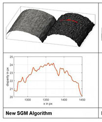
Chromasens, a global leader in linescan machine vision technology, today introduced an advanced 3D reconstruction method to its CS-3D-API (Application Programming Interface) library that empowers integrators to build, deploy, and scale higher value 3D imaging systems capable of improved detection of extremely small defects. Based on the semi-global matching algorithm (SGM), it combines global and local stereo methods for more accurate, pixel-wise matching at low runtime.
Chromasens 3D stereo linescan cameras have been unlocking new insights far beyond the capabilities of standard 2D cameras for over a decade, especially in sectors such as semiconductors and automotive sectors. By measuring the precise location, shape, volume, surface angles and degrees of flatness of objects under inspection at extremely high resolutions, Chromasens 3D cameras ensure manufacturers of defect-free products ranging from ball bearings to fresh fruit.
The new SGM algorithm represents an alternative to the traditional Block Matching (BM) method used previously with Chromasens 3D stereo cameras to match corresponding pixels between two images. The primary difference between the two methods is how a matching cost (energy) is computed. For BM, the cost is computed with normalized cross-correlation, while SGM utilizes a specialized Census transformation. As a result, prior knowledge about a surface structure can be incorporated, making the SGM algorithm more accurate in generating 3D point clouds that better identify object borders, and reconstruct fine structures and weakly textured terrain, without artifacts.
Suggested Items
Driving Innovation: Direct Imaging vs. Conventional Exposure
07/01/2025 | Simon Khesin -- Column: Driving InnovationMy first camera used Kodak film. I even experimented with developing photos in the bathroom, though I usually dropped the film off at a Kodak center and received the prints two weeks later, only to discover that some images were out of focus or poorly framed. Today, every smartphone contains a high-quality camera capable of producing stunning images instantly.
United Electronics Corporation Advances Manufacturing Capabilities with Schmoll MDI-ST Imaging Equipment
06/24/2025 | United Electronics CorporationUnited Electronics Corporation has successfully installed the advanced Schmoll MDI-ST (XL) imaging equipment at their advanced printed circuit board facility. This significant technology investment represents a continued commitment to delivering superior products and maintaining their position as an industry leader in precision PCB manufacturing.
Orbel Corporation Integrates Schmoll Direct Imaging
06/04/2025 | Schmoll AmericaOrbel Corporation in Easton, PA, proudly becomes the first PCM facility in the U.S. equipped with Schmoll’s MDI Direct Imaging system. This installation empowers Orbel to support customers with greater precision and quality.
Key Insights on Photoresist for Defect Reduction
05/21/2025 | I-Connect007 Editorial TeamIn PCB manufacturing, understanding the intricacies of the photoresist process is crucial for achieving high-quality results. Industry experts Josh Krick, a technical service engineer at IEC, and Tim Blair, a PCB imaging specialist at Tim Blair LLC, share their knowledge on the essential stages of photoresist application, highlight critical advancements in materials, and discuss common defects encountered during production. They share best practices and innovative solutions to enhance the manufacturing process, reduce defects, and ensure efficiency and reliability in high-tech applications.
NXP Unveils Third-Generation Imaging Radar Processors for Level 2+ to 4 Autonomous Driving
05/09/2025 | NXP SemiconductorNXP Semiconductors N.V. unveiled its new S32R47 imaging radar processors in 16 nm FinFET technology, building on NXP’s proven expertise in the imaging radar space.