


 The Marketing Minute: AI Is Watching Your Marketing Habits
 Trouble in Your Tank: The Role of Organic Solderability Preservatives in Advanced Packaging
 It’s Only Common Sense: Lighten Up!


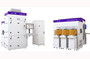
KLA Corporation has announced the Archer™ 750 imaging-based overlay metrology system and the SpectraShape™ 11k optical critical dimension ("CD") metrology system for integrated circuit ("IC" or "chip") manufacturing. As each layer in a chip is constructed, the Archer 750 helps verify that pattern features are correctly aligned to features on previous layers, while the SpectraShape 11k monitors the shapes of three-dimensional structures, such as transistors and memory cells, to ensure they remain in spec. By identifying subtle variations in pattern alignment or feature shape, these new metrology systems help IC manufacturers maintain strict control of the complex processes required to bring high-performance memory and logic chips to market, for applications such as 5G, AI, data centers, and edge computing.
"IC manufacturers are facing process tolerances measured on the atomic scale as they integrate novel structures and new materials into leading-edge chips," said Jon Madsen, senior vice president and general manager of the Metrology division at KLA. "KLA plays a key part in ensuring that these chips can be manufactured cost-effectively with high quality standards. Today I'm proud to announce two additions to our portfolio of metrology solutions, representing the hard work and creative thinking of a top-notch, multi-disciplinary team of engineers and scientists. The new SpectraShape 11k and Archer 750 systems bring much-needed process control capabilities to our fab customers, helping them to produce the innovative electronics that move our world forward."
The Archer 750 overlay metrology system generates accurate and robust measurements of overlay error in the presence of process variation, while achieving productivity levels previously seen only with scatterometry-based overlay systems. This breakthrough system delivers accurate, fast feedback across a range of layers, helping lithographers identify process excursions inline and improve overall patterning integrity, for faster yield ramp and more stable production of advanced logic, DRAM and 3D NAND devices.
The SpectraShape 11k CD and dimensional shape metrology system provides an unprecedented combination of sensitivity and productivity, and accommodates materials, structures and wafer shapes that were previously inaccessible. With its ability to measure advanced logic, DRAM and 3D NAND device features with high precision and speed, the SpectraShape 11k enables quick identification of process issues and rigorous process monitoring during production.
More information about the new metrology systems and the technology advances that enable their enhanced performance can be found on the portfolio information page.
Numerous Archer 750 and SpectraShape 11k systems have been qualified and are in operation at leading IC manufacturers worldwide, where they provide critical feedback for many of the process steps used to produce innovative electronic devices. The Archer 750 and SpectraShape 11k are integrated with KLA's 5D Analyzer® advanced data analysis system, which supports real-time process control, and engineering monitoring and analysis. To maintain the high performance and productivity demanded by chip manufacturers, the Archer 750 and SpectraShape 11k metrology systems are backed by KLA's global comprehensive service network.
About KLA:
KLA develops industry-leading equipment and services that enable innovation throughout the electronics industry. We provide advanced process control and process-enabling solutions for manufacturing wafers and reticles, integrated circuits, packaging, printed circuit boards and flat panel displays. In close collaboration with leading customers across the globe, our expert teams of physicists, engineers, data scientists and problem-solvers design solutions that move the world forward. Additional information may be found at www.kla.com (KLAC-P).


