


 Beyond the Board: What Companies Need to Know Before Entering the MilAero PCB Market
 Defense Speak Interpreted: If CHIPS Cuts Back, What Happens to Electronics Packaging Funds?
 American Made Advocacy: Where’s the Budget for a Modern Military Run on Microelectronics?


RBP Chemical Technology Announces the Release of ONYX™ Direct Metallization System for PCBs
March 11, 2020 | RBP Chemical TechnologyEstimated reading time: 1 minute
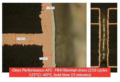
RBP’s ONYX™ is a Direct Metallization System for high reliability and complex printed circuit boards.
The RBP ONYX™ Direct Metallization Process is an integrated system based on a highly conductive form of finely dispersed graphite. Extensively tested and validated, the ONYX™ Process has proven to be versatile and cost effective. Currently the customer base using ONYX™ processes flex, rigid-flex, HDI and high aspect ratio multilayer printed circuit boards with ease and cost effectiveness when compared to conventional electroless copper. The ONYX™ process easily surpasses industry reliability standards including IST (interconnection stress test) and ATC (accelerated thermal cycling).
ONYX™ Direct Metallization System Highlights
The ONYX™ Direct Metallization System is a versatile process and is used in horizontal conveyorized equipment or in vertical immersion mode. Fabricators are able to process a vast array of resin materials including PTFE, polyimide, BT, flex, and basically all epoxy-based resin systems on the market today.
This process is an alternative to electroless copper deposition and provides several significant benefits to the fabricator:
- Less expensive than conventional electroless copper
- Smaller equipment footprint compared to electroless copper
- Greatly reduced water consumption, 4?6 gallons/minute, compared to conventional electroless copper, 26?30 gallons per minute
- ONYX™ contains no chelator as opposed to electroless copper—simplifying waste treatment
About RBP
RBP Chemical Technology is a leading supplier of proprietary chemicals for printed circuit fabrication and semiconductor test applications. RBP’s chemical formulas are tailored to meet the precise needs and requirements for advanced circuit boards, primarily in aerospace, medical and military applications. Headquartered in Milwaukee, Wisconsin and expanding globally, RBP is certified to ISO 9001:2015 and is the Intelligent Choice for the electronics industry.
Share on:


Testimonial
"The I-Connect007 team is outstanding—kind, responsive, and a true marketing partner. Their design team created fresh, eye-catching ads, and their editorial support polished our content to let our brand shine. Thank you all! "
Sweeney Ng - CEE PCBSuggested Items
Trouble in Your Tank: Implementing Direct Metallization in Advanced Substrate Packaging
09/15/2025 | Michael Carano -- Column: Trouble in Your TankDirect metallization systems based on conductive graphite are gaining popularity throughout the world. The environmental and productivity gains achievable with this process are outstanding. Direct metallization reduces the costs of compliance, waste treatment, and legal issues related to chemical exposure. A graphite-based direct plate system has been devised to address these needs.
Closing the Loop on PCB Etching Waste
09/09/2025 | Shawn Stone, IECAs the PCB industry continues its push toward greener, more cost-efficient operations, Sigma Engineering’s Mecer System offers a comprehensive solution to two of the industry’s most persistent pain points: etchant consumption and rinse water waste. Designed as a modular, fully automated platform, the Mecer System regenerates spent copper etchants—both alkaline and acidic—and simultaneously recycles rinse water, transforming a traditionally linear chemical process into a closed-loop system.
Driving Innovation: Depth Routing Processes—Achieving Unparalleled Precision in Complex PCBs
09/08/2025 | Kurt Palmer -- Column: Driving InnovationIn PCB manufacturing, the demand for increasingly complex and miniaturized designs continually pushes the boundaries of traditional fabrication methods, including depth routing. Success in these applications demands not only on robust machinery but also sophisticated control functions. PCB manufacturers rely on advanced machine features and process methodologies to meet their precise depth routing goals. Here, I’ll explore some crucial functions that empower manufacturers to master complex depth routing challenges.
Trouble in Your Tank: Minimizing Small-via Defects for High-reliability PCBs
08/27/2025 | Michael Carano -- Column: Trouble in Your TankTo quote the comedian Stephen Wright, “If at first you don’t succeed, then skydiving is not for you.” That can be the battle cry when you find that only small-diameter vias are exhibiting voids. Why are small holes more prone to voids than larger vias when processed through electroless copper? There are several reasons.
The Government Circuit: Navigating New Trade Headwinds and New Partnerships
08/25/2025 | Chris Mitchell -- Column: The Government CircuitAs global trade winds continue to howl, the electronics manufacturing industry finds itself at a critical juncture. After months of warnings, the U.S. Government has implemented a broad array of tariff increases, with fresh duties hitting copper-based products, semiconductors, and imports from many nations. On the positive side, tentative trade agreements with Europe, China, Japan, and other nations are providing at least some clarity and counterbalance.