


 The Hidden Enabler of Autonomous Warfare: Advanced PCB Technologies Behind Defense AI
 It’s Only Common Sense: Stay Curious, My Friends


Marking a new phase of its strategy to serve customers in the precision optics industry, SOLAYER reported today that it is now mass-producing standardized models of its high-precision coating tools. The company is an innovator of plasma-based surface treatment technology solutions for manufacturers of special glass and photonics products used to enable 3D sensors, telecommunications, LIDAR, and other applications. SOLAYER’s tools, like the flagship AVIOR M-300 sputtering system, can deposit a vast range of ultra-thin films with extraordinary precision. They deliver excellent film uniformity with high reliability in volume production, at a low cost-of-ownership. In due course, the company will also serve semiconductor customers.
Since 2007, SOLAYER has focused on developing specialized coating technologies for research and pilot lines, as well as mass production. The technologies include plasma pre-treatment, magnetron sputtering, PECVD, and RTP through flash lamp annealing. In 2016, the company started developing products for the photonics market, first offering customized tools for specialized production lots, and now standardized systems for mass production. In late 2019, SOLAYER drew financing from a strategic investor in China.
Sputtered Films: Enabling Innovation for Photonics Applications
As photonics products grow more sophisticated, the manufacturing requirements are more stringent. In particular, the coating specifications for optical films are more complex, and the quality expectations are high. Advanced sputtering has emerged as an ideal technique for its capability to generate films with high density, better stability, high uniformity, and minimal optical losses. The shift-free structure makes for predictable mechanical strength under stress conditions—which reinforces quality.
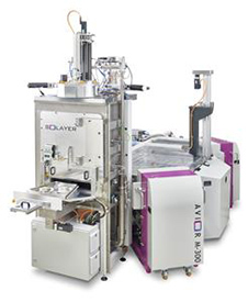
Modular, Scalable Optical Coating Solutions for Flexibility, Productivity and Performance
SOLAYER’s fully automated optical coating tools are built to address the manufacturing imperatives. Featuring modular, scalable platforms, they are engineered for easy ramp-up, as well as maximum flexibility and uptime. The company’s premier tool, the AVIOR M-300 system, is equipped for volume production on substrates up to 300mm. Its sputter-up, substrate-facedown configuration virtually eliminates particles while delivering a reproducible coating process with extended stability. Target material utilization is approximately 85 percent (silicon, niobium, tantalum and amorphous silicon oxides, etc.), and throughput is nearly 50 percent higher (24’ x 200 mm substrates) than competitive tools.
“We’re excited to reach this mass-production milestone,” said SOLAYER’s CEO, Mathias Hoefler. “Our tools are the result of extensive research and development, and built with German-engineered ingenuity in the heart of Silicon Saxony. Beyond the performance, throughput and yield advantages, they offer superior cost benefits to customers manufacturing cutting-edge precision optics products with very complex coating requirements.”
SOLAYER tools are further differentiated by components developed and qualified specifically for use in the optical industry. For customers, this means specialized tools with custom parts that combine to enable extremely reliable and cost-effective coating processes.
In addition to the AVIOR M-300 system, SOLAYER’s optical coating solutions also include the ALASCO, a modular cluster coating tool, and the ALIOTH, a versatile inline coating system, offering a complete portfolio for customers’ diverse needs.


