


 Global PCB Connections: Rigid-flex and Flexible PCBs—The Backbone of Modern Electronics
 Flexible Thinking: The Key to a Successful Flex Circuit Design Transfer
 Happy’s Tech Talk #29: Bend-to-Install Semi-flex FR-4


Nano Dimension and Piezoskin Developed a Customized 3D-Printed MEMS Package with Electric Pads
April 15, 2020 | Nano Dimension Ltd.Estimated reading time: Less than a minute
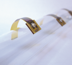
Nano Dimension Ltd., a leading Printed electronics (PE) / Additively Manufactured Electronics (AME) provider, announced today that its technology, DragonFly LDM system and materials were used to develop a 3D printed sealed packaging with electrical pads for Micro-Electromechanical Systems (MEMS).
The printed electronics package has the electrical pads directly printed on the metal layers on which an RF connector is soldered. The ability to transfer electric pads in a sealed package is one of the most crucial parts in ohmic-contact microelectromechanical systems (MEMS) as it determines the device performance and reliability, particularly for soft and flexible devices where the electrical connectors are typically difficult to produce.
“Nano Dimension’s AME technology helped us to achieve an original product prototype in which wires and connectors were eliminated such that the package was minimized to obtain an optimal user experience. It simplifies the manufacturing process compared to traditional manufacturing methods,” said Dr. Francesco Guido, CTO of Piezoskin S.R.L.
“With the DragonFly LDM 3D printer, Piezoskin can design customized printedpackages with flexible transducers, to meet their customers unique needs, drive innovation and get products to market faster,” said Mr. Yoav Stern, Nano Dimension’s CEO and President.
Share on:


Testimonial
"We’re proud to call I-Connect007 a trusted partner. Their innovative approach and industry insight made our podcast collaboration a success by connecting us with the right audience and delivering real results."
Julia McCaffrey - NCAB GroupSuggested Items
DARPA, State of New Mexico Establish Framework to Advance Quantum Computing
09/08/2025 | DARPAAs part of the Quantum Benchmarking Initiative (QBI), DARPA signed an agreement with the State of New Mexico’s Economic Development Department to create the Quantum Frontier Project.
LPKF Strengthens LIDE Technology Leadership with New Patent Protection in Korea
09/04/2025 | LPKFLPKF Laser & Electronics SE today announced that its groundbreaking LIDE (Laser Induced Deep Etching) technology has received additional patent protection in Korea through the Korean Patent Office (KPCA), effective September 1, 2025.
UHDI Fundamentals: UHDI Technology and Industry 4.0
09/03/2025 | Anaya Vardya, American Standard CircuitsUltra high density interconnect (UHDI) technology is rapidly transforming how smart systems are designed and deployed in the context of Industry 4.0. With its capacity to support highly miniaturized, high-performance, and densely packed electronics, UHDI is a critical enabler of the smart, connected, and automated industrial future. Here, I’ll explore the synergy between UHDI and Industry 4.0 technologies, highlighting applications, benefits, and future directions.
CEE PCB Launches PCBpedia: A New Knowledge Hub for Circuit Board Technology
09/03/2025 | CEE PCBCEE PCB, a leading manufacturer of PCBs and FPCs, is responding to the growing demand for reliable technical knowledge. With PCBpedia, CEE introduces a new knowledge platform featuring expert articles on key topics in circuit board technology – from FPC design rules to surface finishes.
Coming Soon: The Advanced Electronics Packaging Digest
08/27/2025 | Marcy LaRont, I-Connect007The upcoming Advanced Electronics Packaging Digest is a curated, condensed monthly publication designed to keep you informed and engaged with the fast-moving world of advanced electronics packaging (AEP). In our inaugural September issue, we will begin at the foundation with an in-depth interview featuring Matt Kelly, CTO of the Global Electronics Association. Kelly and his Technology Solutions Team approach advanced packaging from a holistic systems perspective.