


 Defense Speak Interpreted: If CHIPS Cuts Back, What Happens to Electronics Packaging Funds?
 American Made Advocacy: Where’s the Budget for a Modern Military Run on Microelectronics?
 Beyond the Board: Orbital High Ground—Why Space Superiority Is Slipping Away


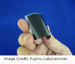
Fujitsu Successfully Develops Flexible Nanotube Adhesive Sheet Technology with High Thermal Conductivity
April 20, 2020 | Fujitsu Laboratories LtdEstimated reading time: 4 minutes
Fujitsu Laboratories Ltd. today announced the development of the world's first adhesive sheet composed of carbon nanotubes with extremely high thermal conductivity of up to 100 W/mK (watt per meter per Kelvin).
Carbon nanotubes have high thermal conductivity and represent a promising candidate for heat dissipation from heat sources including semiconductor devices. Nevertheless, the material remains difficult to handle due to its fragility, rendering it impractical for many purposes. To address this, Fujitsu has successfully developed a technology for laminating vertically aligned carbon nanotubes, while maintaining their original characteristics of high thermal conductivity and flexibility, as well as a technology for bonding them with sufficient adhesion. This technology facilitates the cutting and handling of carbon nanotube sheets, making it possible to use them as a heat dissipation material, for example, in automotive power modules for electric vehicles (EVs).
Fujitsu aims to license the use of its newly-developed carbon nanotube adhesive sheets to companies in the materials and electrical industries, and will continue to support their use in a variety of commercial applications.
Background and Development
EVs are increasingly being put to practical use as efforts to regulate greenhouse gases accelerate throughout the world. Despite this, the fact that EVs are more expensive than gasoline-powered vehicles and lack similar driving ranges continues to hinder their widespread adoption.
In order to improve cost-performance and driving range in recent years, efforts have been made to develop semiconductor devices that use silicon carbide or gallium nitride as an alternative material to the more commonly-used silicon to reduce the size, weight, power consumption, and cost of power modules for electric vehicles. In order to make this a reality, however, countermeasures to deal with heat generated around semiconductor devices due to module miniaturization must be resolved, and components such as heat dissipation materials and bonding materials that make up modules must be designed to achieve unprecedented levels of heat resistance and thermal conductivity.
Challenges
Carbon nanotubes, a type of nanotechnology material made from carbon atoms, have thermal conductivity that is about 10 times higher than copper. One potential use of this material is its use as a heat sink for dissipating heat from heat sources like semiconductor devices. In 2017, Fujitsu developed a high thermal conductivity sheet using carbon nanotubes, but in order to maintain the sheet shape, the sheet is sintered and molded at an ultra-high temperature of 2000 °C or higher, which results in a material that is inflexible. A hard sheet can be attached to flat materials, but it is not suitable for joining materials together that are uneven, which inhibits the places in which the sheet can be applied.
Furthermore, in areas around semiconductor devices where reliability is essential, it is necessary to bond both the semiconductor and heatsink via a heat dissipation sheet consisting of carbon nanotubes in order to follow the change in shape caused by temperature differences before and after the device is operated. In general, carbon nanotubes are made adhesive by mixing them into an adhesive material such as resin or rubber, forming a sheet. However, because these adhesive materials have low thermal conductivity, it has been extremely difficult to achieve sufficient levels of both thermal conductivity and adhesion.
About the Newly Developed Technology
Fujitsu has developed the world's first carbon nanotube adhesive sheet that exhibits extremely high thermal conductivity of up to 100 W/mK even when interface resistance is included.
The features of the developed technology are as follows.
- Sheet Laminate Technology Fujitsu has developed a technique for laminating vertically aligned carbon nanotubes while maintaining the alignment. The laminate layer consists of two layers, a protective sheet and an adhesive layer, and has a laminate structure in which the laminate layer protects the top and bottom of carbon nanotubes. Carbon nanotubes are difficult to use as heat dissipating materials because they easily lose their shape. However, this technology protects the carbon nanotubes themselves with a laminate layer, making them stable in shape and making cutting and handling easier, which was difficult with conventional technologies.
Figure1: Internal structure of carbon nanotube adhesive sheet
- High-Thermal-Conductivity Sheet Bonding Technology The adhesive layer that makes up the laminate layer is made of a polymer that is several microns thick. Because even a small amount of resin can cause large thermal resistance, it has become an issue that must be solved to achieve both adhesiveness and thermal conductivity. Thus, by optimizing three or more correlation parameters, such as the density of carbon nanotubes, the type and thickness of the resin, and the bonding conditions, utilizing knowledge of thermal resistance at the interface between carbon nanotubes and resins cultivated over many years, it becomes possible to bond carbon nanotubes while maintaining sufficient adhesive properties without impairing thermal conductivity.
Effects
The newly developed carbon nanotube adhesive sheet has thermal conductivity of up to 3 times that of the conventional indium heat dissipation material, which is known as a high thermal conductivity material, compared with measured values including interface resistance.
Since the sheet is laminated with adhesive and protective layers, it can be easily cut and handled, and can be used for applications requiring adhesion.
These technologies will make it possible to put carbon nanotubes into practical use as heat dissipating materials, including in automotive power modules for EVs.
Future Plans
Going forward, Fujitsu Laboratories will license the use of its carbon nanotube adhesive sheets to companies in the materials and electrical industries. and will continue to support their commercialization and practical use.
Share on:


Testimonial
"We’re proud to call I-Connect007 a trusted partner. Their innovative approach and industry insight made our podcast collaboration a success by connecting us with the right audience and delivering real results."
Julia McCaffrey - NCAB GroupSuggested Items
Driving Innovation: Depth Routing Processes—Achieving Unparalleled Precision in Complex PCBs
09/08/2025 | Kurt Palmer -- Column: Driving InnovationIn PCB manufacturing, the demand for increasingly complex and miniaturized designs continually pushes the boundaries of traditional fabrication methods, including depth routing. Success in these applications demands not only on robust machinery but also sophisticated control functions. PCB manufacturers rely on advanced machine features and process methodologies to meet their precise depth routing goals. Here, I’ll explore some crucial functions that empower manufacturers to master complex depth routing challenges.
Trouble in Your Tank: Minimizing Small-via Defects for High-reliability PCBs
08/27/2025 | Michael Carano -- Column: Trouble in Your TankTo quote the comedian Stephen Wright, “If at first you don’t succeed, then skydiving is not for you.” That can be the battle cry when you find that only small-diameter vias are exhibiting voids. Why are small holes more prone to voids than larger vias when processed through electroless copper? There are several reasons.
The Government Circuit: Navigating New Trade Headwinds and New Partnerships
08/25/2025 | Chris Mitchell -- Column: The Government CircuitAs global trade winds continue to howl, the electronics manufacturing industry finds itself at a critical juncture. After months of warnings, the U.S. Government has implemented a broad array of tariff increases, with fresh duties hitting copper-based products, semiconductors, and imports from many nations. On the positive side, tentative trade agreements with Europe, China, Japan, and other nations are providing at least some clarity and counterbalance.
How Good Design Enables Sustainable PCBs
08/21/2025 | Gerry Partida, Summit InterconnectSustainability has become a key focus for PCB companies seeking to reduce waste, conserve energy, and optimize resources. While many discussions on sustainability center around materials or energy-efficient processes, PCB design is an often overlooked factor that lies at the heart of manufacturing. Good design practices, especially those based on established IPC standards, play a central role in enabling sustainable PCB production. By ensuring designs are manufacturable and reliable, engineers can significantly reduce the environmental impact of their products.
50% Copper Tariffs, 100% Chip Uncertainty, and a Truce
08/19/2025 | Andy Shaughnessy, I-Connect007If you’re like me, tariffs were not on your radar screen until a few months ago, but now political rhetoric has turned to presidential action. Tariffs are front-page news with major developments coming directly from the Oval Office. These are not typical times. President Donald Trump campaigned on tariff reform, and he’s now busy revamping America’s tariff policy.