-
-
News
News Highlights
- Books
Featured Books
- smt007 Magazine
Latest Issues
Current IssueProduction Software Integration
EMS companies need advanced software systems to thrive and compete. But these systems require significant effort to integrate and deploy. What is the reality, and how can we make it easier for everyone?
Spotlight on India
We invite you on a virtual tour of India’s thriving ecosystem, guided by the Global Electronics Association’s India office staff, who share their insights into the region’s growth and opportunities.
Supply Chain Strategies
A successful brand is built on strong customer relationships—anchored by a well-orchestrated supply chain at its core. This month, we look at how managing your supply chain directly influences customer perception.
- Articles
- Columns
- Links
- Media kit
||| MENU - smt007 Magazine
Indium Corporation Engineers Earn SMTA Certification
June 25, 2020 | Indium CorporationEstimated reading time: 1 minute

Indium Corporation is proud to announce that members of its United States-based technical support team have earned SMTA certification.
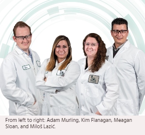
Two Technical Support Engineers have recently earned certification as Certified SMT Process Engineers (CSMTPE): Meagan Sloan and Miloš Lazi?.
They join a number of CSMTPE colleagues at Indium Corporation, including two fellow United States-based technical support team members: Adam Murling, Technical Support Engineer II and Lean Six Sigma Green Belt; and Kimberly Flanagan, Technical Support Engineer II.
SMTA's CSMTPE Certification is a unique program that is sponsored by the Surface Mount Technology Association (SMTA), which recognizes and certifies competence across the entire SMT assembly process at an engineering level. This certification is one of the electronics assembly industry's most respected validations of process excellence.
Indium Corporation is a premier materials manufacturer and supplier to the global electronics, semiconductor, thin-film, and thermal management markets. Products include solders and fluxes; brazes; thermal interface materials; sputtering targets; indium, gallium, germanium, and tin metals and inorganic compounds; and NanoFoil®. Founded in 1934, the company has global technical support and factories located in China, India, Malaysia, Singapore, South Korea, the United Kingdom, and the USA.
For more information about Indium Corporation, visit www.indium.com or email jhuang@indium.com. You can also follow our experts, From One Engineer To Another® (#FOETA), at www.facebook.com/indium or @IndiumCorp.
Testimonial
"Advertising in PCB007 Magazine has been a great way to showcase our bare board testers to the right audience. The I-Connect007 team makes the process smooth and professional. We’re proud to be featured in such a trusted publication."
Klaus Koziol - atgSuggested Items
Taking Control of PCB Verification One Step at a Time
10/09/2025 | Kirk Fabbri, Siemens EDAToday’s designs are as complex as ever, and engineers face tough decisions every day. Simulation and verification teams are confronted with a three-fold challenge: understanding the underlying theory, mastering the tools, and applying best practices.Engineers need to navigate a vast and ever-changing cast of design and simulation tools, often with overlapping functionality.
Happy’s Tech Talk #43: Engineering Statistics Training With Free Software
10/06/2025 | Happy Holden -- Column: Happy’s Tech TalkIn over 50 years as a PCB process engineer, the one skill I acquired in college that has been most beneficial is engineering statistics. Basic statistics was part of my engineering fundamentals classes, but I petitioned the dean to let me take the engineering statistics graduate course because I was creating a senior thesis for my honors focus and needed more training on Design of Experiments (DOE).
Connect the Dots: Evolution of PCB Manufacturing—Lamination
10/02/2025 | Matt Stevenson -- Column: Connect the DotsWhen I wrote The Printed Circuit Designer's Guide to...™ Designing for Reality, it was not a one-and-done effort. Technology is advancing rapidly. Designing for the reality of PCB manufacturing will continue to evolve. That’s why I encourage designers to stay on top of the tools and processes used during production, to ensure their designs capitalize on the capabilities of their manufacturing partner.
Empower Sets New Benchmark with 20x Faster Response and Breakthrough Sustainability Demonstrated at OCP Global Summit 2025
09/25/2025 | Empower SemiconductorEmpower Semiconductor, the world leader in powering AI-class processors, announced that its Crescendo chipset, an artificial intelligence (AI) and high-performance computing (HPC) processor true vertical power delivery platform, is available now for final sampling, with mass production slated for late 2025.
Driving Innovation: Mastering Panel Warpage
09/23/2025 | Simon Khesin -- Column: Driving InnovationDuring the complex and multi-step process of PCB fabrication, a panel's flatness is constantly at risk. A host of factors can introduce warpage, bending, and unevenness, presenting a fundamental challenge to achieving high-precision results. This deformation (sometimes referred to as “bow and twist”), even on a microscopic scale, can lead to critical defects during subsequent stages, such as component surface mounting (e.g., tombstoning, solder opens) and the PCB's long-term functional reliability.