-

- News
- Books
Featured Books
- smt007 Magazine
Latest Issues
Current Issue
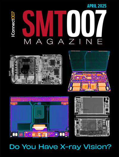
Do You Have X-ray Vision?
Has X-ray’s time finally come in electronics manufacturing? Join us in this issue of SMT007 Magazine, where we answer this question and others to bring more efficiency to your bottom line.

IPC APEX EXPO 2025: A Preview
It’s that time again. If you’re going to Anaheim for IPC APEX EXPO 2025, we’ll see you there. In the meantime, consider this issue of SMT007 Magazine to be your golden ticket to planning the show.

Technical Resources
Key industry organizations–all with knowledge sharing as a part of their mission–share their technical repositories in this issue of SMT007 Magazine. Where can you find information critical to your work? Odds are, right here.
- Articles
- Columns
Search Console
- Links
- Media kit
||| MENU - smt007 Magazine
Samsung Leads Semiconductor Paradigm Shift with New Material Discovery
July 7, 2020 | SamsungEstimated reading time: 1 minute
Researchers at the Samsung Advanced Institute of Technology (SAIT) have unveiled the discovery of a new material, called amorphous boron nitride (a-BN), in collaboration with Ulsan National Institute of Science and Technology (UNIST) and the University of Cambridge. Published in the journal Nature, the study has the potential to accelerate the advent of the next generation of semiconductors.
2D Materials – The Key to Overcoming Scalability Challenges
Recently, SAIT has been working on the research and development of two-dimensional (2D) materials – crystalline materials with a single layer of atoms. Specifically, the institute has been working on the research and development of graphene, and has achieved groundbreaking research outcomes in this area such as the development of a new graphene transistor as well as a novel method of producing large-area, single-crystal wafer-scale graphene. In addition to researching and developing graphene, SAIT has been working to accelerate the material’s commercialization.
“To enhance the compatibility of graphene with silicon-based semiconductor processes, wafer-scale graphene growth on semiconductor substrates should be implemented at a temperature lower than 400°C.” said Hyeon-Jin Shin, a graphene project leader and Principal Researcher at SAIT. “We are also continuously working to expand the applications of graphene beyond semiconductors.”
2D Material Transformed – Amorphous Boron Nitride
The newly discovered material, called amorphous boron nitride (a-BN), consists of boron and nitrogen atoms with an amorphous molecule structure. While amorphous boron nitride is derived from white graphene, which includes boron and nitrogen atoms arranged in a hexagonal structure, the molecular structure of a-BN in fact makes it uniquely distinctive from white graphene.
Amorphous boron nitride has a best-in-class ultra-low dielectric constant of 1.78 with strong electrical and mechanical properties, and can be used as an interconnect isolation material to minimize electrical interference. It was also demonstrated that the material can be grown on a wafer scale at a low temperature of just 400°C. Thus, amorphous boron nitride is expected to be widely applied to semiconductors such as DRAM and NAND solutions, and especially in next generation memory solutions for large-scale servers.
“Recently, interest in 2D materials and the new materials derived from them has been increasing. However, there are still many challenges in applying the materials to existing semiconductor processes.” said Seongjun Park, Vice President and Head of Inorganic Material Lab, SAIT. “We will continue to develop new materials to lead the semiconductor paradigm shift.”
Suggested Items
DuPont Announces Additional Directors for the Planned Independent Electronics Company
04/18/2025 | DuPontDuPont announced that Karin De Bondt and Anne Noonan will become members of the future board of directors for the independent Electronics public company that will be created following its intended spin-off from DuPont, which is targeted for November 1, 2025.
Indium Experts to Present on Power Electronics at PCIM Europe 2025
04/17/2025 | Indium CorporationAs one of the leading materials providers to the power electronics assembly and e-Mobility industries, Indium Corporation experts will share their technical insight and knowledge on a variety of industry-related topics throughout PCIM Europe, May 6-8, in Nuremberg, Germany.
YINCAE to Showcase Cutting-Edge Solutions at SEMICON Southeast Asia 2025
04/16/2025 | YINCAEYINCAE Advanced Materials, a leading provider of innovative solutions for the semiconductor and microelectronics industries, is proud to announce its participation in SEMICON Southeast Asia 2025.
Improve Your Process Reliability: Axxon-Mycronic and HumiSeal to Host Conformal Coating Workshop in Guadalajara
04/15/2025 | Axxon-MycronicAxxon-Mycronic, a leading, global supplier of innovative and production-ready, dispensing and conformal coating systems, in collaboration with HumiSeal, a global expert in protective coating materials, is excited to announce a Conformal Coating Workshop taking place on May 8, 2025 in Guadalajara, Mexico.
Real Time with... IPC APEX EXPO 2025: Exploring LCP Materials with Matrix Electronics
04/15/2025 | Real Time with...IPC APEX EXPONolan Johnson introduces Robert Berg from Matrix Electronics, highlighting the company's focus on high-speed, low-loss flexible materials, especially LCP materials. LCP (liquid crystal polymer) is a thermal plastic with unique properties that make it ideal for advanced PCB applications. Despite processing challenges, its stability and FDA approval for medical use drive interest in aerospace and medical markets.


