


 Knocking Down the Bone Pile: The Business Case for Component Reclamation
 Global Sourcing Spotlight: The Hidden Power of the Rep Network
 Smart Automation: When Traditional Depaneling Methods Reach Their Limits


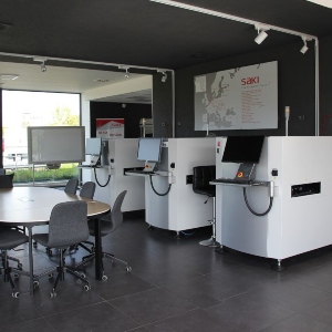
Saki Corporation, an innovator in the field of automated optical and X-ray inspection equipment, announces the expansion of the new EMEA regional head office in Prague (Czech Republic) with the opening of a brand-new Solution Center. The new 650m2 Solution Center showcases Saki's latest 3D SPI, 2D/3D AOI and AXI systems as well as inspection solutions using optional software. A comprehensive in-house and online machine operation training program is also offered.
The offices of Saki EU (Saki Europe GmbH, European sales and service subsidiary of Saki Corporation) relocated to larger premises in Prague, Czech Republic in 2019, offering approximately three times the area of the previous office. 650m2 of the facility has been dedicated to a brand-new Solution Center. This is the first large-scale Solution Center of its kind for the EMEA region where customers can experience the capabilities of Saki's latest lineup of diverse equipment and inspection solutions, and advanced M2M capabilities, including:
- 3Si-LS2: Saki's high-precision and high-speed 3D solder paste inspection machine (3D SPI). The single-lane system is equipped with a 12µm camera head for board sizes from 50mm×60mm to 500mm×510mm.
- 3Di-LS2: a single lane 3D automated optical inspection (AOI) solution with camera resolution levels of 12µm and 18µm. The machine is equipped with a quad side camera system that ensures inspection of the entire board, including dead angles and areas missed by overhead cameras.
- 2Di?LU1: an inline bottom-side automated optical inspection (AOI) system. Saki's 2D line-scan technology is ultra-fast, capturing the image of an entire 460x500mm printed circuit board assembly (PCBA) and carriers of 610x610mm in one pass, in real time. This versatile system automates the bottom-side inspection process, eliminates board flipping and handling, and ensures quality after the potting, dip, wave, and selective soldering processes.
- 3Xi-M110: Saki's compact, lightweight, inline 3D-CT automated X-ray inspection (AXI) machine for printed circuit board assemblies that ensures the quality of hidden solder joints for bottom-electrode packages such as BGAs, LGAs, QFNs, flip-chip, and package-on-package and provides precise volumetric measurements and shape reconstruction to find voids, head-in-pillow, and other defects that are difficult to identify.
- 2D AOI, BF-Sirius and all 3D AOI generations, 3Di series, 3Di-L1 series are also installed for full customer support, software development and testing.
- Full optional lineup at the center: Offline Teaching station (BF2-Editor), Verification station (BF2-Monitor), Multi Process View and QD Analyzer beta version for advanced SPC.
The center also hosts a comprehensive program of machine operator, programming, and service & machine maintenance training courses for customers and distributors. Furthermore Saki continues to expand a choice of online training and demonstration solutions which offer a convenient and easy-to-access option for customers who are unable to visit the Solution Center and in light of the current restrictions on movement due to the coronavirus pandemic.
Mr Jarolslav Neuhauser, General Manager of Saki EU commented: “The new Saki Solution Center in Prague provides a great inspection technology showcase with increased training capacity for our customers and partners. Our investment demonstrates our continued long-term commitment to the EMEA region and addresses the diverse training demands of our customers & distributors. I look forward to welcoming them to Prague.”


