Atotech to Present at 17th International Wafer-Level Packaging Conference 2020
October 9, 2020 | AtotechEstimated reading time: Less than a minute

Atotech, a leading global provider of electroplating and surface-finishing chemicals and equipment for PCB, semiconductor advanced packaging and dual damascene applications, will present at this year’s IWLPC. The on-demand conference and expo will be held from October 13th through 30th.
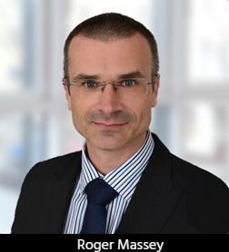
Atotech’s expert, Roger Massey, will give a technical paper presentation entitled “Hydrogen embrittlement and nano void classification within electroless copper depositions”. His presentation is part of the 3D Integration track and will be available for viewing during the entire time the conference is open. Attendees of this virtually held conference are invited to watch Mr. Massey’s presentation.
For more information about Atotech or its product offering, please visit www.atotech.com or contact us at: info@atotech.com.
About Atotech
Atotech is a global leader in surface-finishing solutions. Through a comprehensive systems-and-solutions approach, the company delivers chemistry, equipment, and service to support diverse industries such as consumer electronics, especially mobile devices and computing; global automotive; communication infrastructure; and many other industrial end-markets. Atotech’s relentless R&D efforts and global TechCenter presence allows it to deliver pioneering and sustainable products combined with unparalleled on-site customer support – making Atotech a critical partner to over 8,000 customers worldwide.
Suggested Items
I-Connect007 Editor’s Choice: Five Must-Reads for the Week
07/18/2025 | Nolan Johnson, I-Connect007It may be the middle of the summer, but the news doesn’t quit, and there’s plenty to talk about this week, whether you’re talking technical or on a global scale. When I have to choose six items instead of my regular five, you know it’s good. I start by highlighting my interview with Martyn Gaudion on his latest book, share some concerning tariff news, follow that up with some promising (and not-so-promising) investments, and feature a paper from last January’s inaugural Pan-European Design Conference.
Elephantech Launches World’s Smallest-Class Copper Nanofiller
07/17/2025 | ElephantechJapanese deep-tech startup Elephantech has launched its cutting-edge 15 nm class copper nanofiller – the smallest class available globally. This breakthrough makes Elephantech one of the first companies in the world to provide such advanced material for commercial use.
Copper Price Surge Raises Alarms for Electronics
07/15/2025 | Global Electronics Association Advocacy and Government Relations TeamThe copper market is experiencing major turbulence in the wake of U.S. President Donald Trump’s announcement of a 50% tariff on imported copper effective Aug. 1. Recent news reports, including from the New York Times, sent U.S. copper futures soaring to record highs, climbing nearly 13% in a single day as manufacturers braced for supply shocks and surging costs.
I-Connect007 Editor’s Choice: Five Must-Reads for the Week
07/11/2025 | Andy Shaughnessy, Design007 MagazineThis week, we have quite a variety of news items and articles for you. News continues to stream out of Washington, D.C., with tariffs rearing their controversial head again. Because these tariffs are targeted at overseas copper manufacturers, this news has a direct effect on our industry.I-Connect007 Editor’s Choice: Five Must-Reads for the Week
Digital Twin Concept in Copper Electroplating Process Performance
07/11/2025 | Aga Franczak, Robrecht Belis, Elsyca N.V.PCB manufacturing involves transforming a design into a physical board while meeting specific requirements. Understanding these design specifications is crucial, as they directly impact the PCB's fabrication process, performance, and yield rate. One key design specification is copper thieving—the addition of “dummy” pads across the surface that are plated along with the features designed on the outer layers. The purpose of the process is to provide a uniform distribution of copper across the outer layers to make the plating current density and plating in the holes more uniform.