


 It’s Only Common Sense: If You’re Not Differentiated, You’re Dead
 Alpha Insights, Performance by Design: The Future of PCB Manufacturing in the Midwest
 Happy’s Tech Talk #43: Engineering Statistics Training With Free Software


Applied Materials, BE Semiconductor Industries to Accelerate Chip Integration Technology
October 22, 2020 | Globe NewswireEstimated reading time: 2 minutes
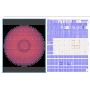
Applied Materials, Inc. and BE Semiconductor Industries N.V. announced an agreement to develop the industry’s first complete and proven equipment solution for die-based hybrid bonding, an emerging chip-to-chip interconnect technology that enables heterogeneous chip and subsystem designs for applications including high-performance computing, AI and 5G.
As traditional 2D scaling slows, the semiconductor industry is shifting towards heterogeneous design and chip integration as a new way to deliver improvements in performance, power, area/cost and time-to-market (PPACt). To accelerate this trend, Applied and Besi have formed a joint development program and are establishing a Center of Excellence focused on next-generation chip-to-chip bonding technology. The program harnesses the companies’ respective front- and back-end semiconductor expertise to deliver co-optimized integrated hybrid bonding configurations and equipment solutions for customers.
“Challenges in conventional Moore’s Law scaling are straining the economics and pace of the semiconductor industry’s roadmap,” said Nirmalya Maity, Corporate Vice President of Advanced Packaging at Applied Materials. “Our collaboration with Besi and the formation of a new Hybrid Bonding Center of Excellence are key components of Applied’s strategy to equip customers with a ‘New Playbook’ for driving improvements in PPACt. Applied looks forward to working with Besi to co-optimize our equipment offerings and accelerate advanced heterogeneous integration technology for our customers.”
“We are excited about forming this unique joint development program with Applied Materials which brings together the semiconductor industry’s leading materials engineering and advanced packaging technologies for customers,” said Ruurd Boomsma, CTO of Besi. “Our collaboration can greatly accelerate the adoption and proliferation of hybrid bonding for leading-edge 5G, AI, high-performance computing, data storage and automotive applications.”
Hybrid bonding connects multiple “chiplets” in die form using direct, copper interconnects. This technique enables designers to bring chiplets of various process nodes and technologies into closer physical and electrical proximity so that they perform as well or better than if they were made on a single large, monolithic die. Hybrid bonding is a major improvement over conventional chip packaging because it permits increased chip density and shortens the lengths of the interconnect wiring between chiplets, thereby improving overall performance, power, efficiency and cost.
A complete die-based hybrid bonding equipment solution requires a broad suite of semiconductor manufacturing technologies along with high-speed and extremely precise chiplet placement technology. To achieve this, the joint development program brings together Applied’s semiconductor process expertise in etch, planarization, deposition, wafer cleaning, metrology, inspection and particle defect control with Besi’s leading die placement, interconnect and assembly solutions.
The Center of Excellence will be located at Applied’s Advanced Packaging Development Center in Singapore which is one of the industry’s most advanced wafer-level packaging labs. It enables the foundational building blocks of heterogenous integration in a 17,300-square-foot Class 10 cleanroom with full lines of wafer-level packaging equipment. The Center of Excellence will provide customers a platform to accelerate the development of custom hybrid bonding test vehicles including design, modeling, simulation, fabrication and testing.
Share on:


Testimonial
"Advertising in PCB007 Magazine has been a great way to showcase our bare board testers to the right audience. The I-Connect007 team makes the process smooth and professional. We’re proud to be featured in such a trusted publication."
Klaus Koziol - atgSuggested Items
Nolan’s Notes: Tariffs, Technologies, and Optimization
10/01/2025 | Nolan Johnson -- Column: Nolan's NotesLast month, SMT007 Magazine spotlighted India, and boy, did we pick a good time to do so. Tariff and trade news involving India was breaking like a storm surge. The U.S. tariffs shifted India from one of the most favorable trade agreements to the least favorable. Electronics continue to be exempt for the time being, but lest you think that we’re free and clear because we manufacture electronics, steel and aluminum are specifically called out at the 50% tariff levels.
MacDermid Alpha & Graphic PLC Lead UK’s First Horizontal Electroless Copper Installation
09/30/2025 | MacDermid Alpha & Graphic PLCMacDermid Alpha Electronics Solutions, a leading supplier of integrated materials and chemistries to the electronics industry, is proud to support Graphic PLC, a Somacis company, with the installation of the first horizontal electroless copper metallization process in the UK.
Electrodeposited Copper Foils Market to Grow by $11.7 Billion Over 2025-2032
09/18/2025 | Globe NewswireThe global electrodeposited copper foils market is poised for dynamic growth, driven by the rising adoption in advanced electronics and renewable energy storage solutions.
MacDermid Alpha Showcases Advanced Interconnect Solutions at PCIM Asia 2025
09/18/2025 | MacDermid Alpha Electronics SolutionsMacDermid Alpha Electronic Solutions, a global leader in materials for power electronics and semiconductor assembly, will showcase its latest interconnect innovations in electronic interconnect materials at PCIM Asia 2025, held from September 24 to 26 at the Shanghai New International Expo Centre, Booth N5-E30
Trouble in Your Tank: Implementing Direct Metallization in Advanced Substrate Packaging
09/15/2025 | Michael Carano -- Column: Trouble in Your TankDirect metallization systems based on conductive graphite are gaining popularity throughout the world. The environmental and productivity gains achievable with this process are outstanding. Direct metallization reduces the costs of compliance, waste treatment, and legal issues related to chemical exposure. A graphite-based direct plate system has been devised to address these needs.