


 Dan’s Biz Bookshelf: 'This Is Strategy: Make Better Plans'
 The Chemical Connection: Reducing Defects in Circuit Board Production
 It’s Only Common Sense: Trust Is All You Need


Real Time with… Altium Live Europe 2020: Rick Hartley’s Secrets of PCB Optimization
October 29, 2020 | Pete Starkey, I-Connect007Estimated reading time: 4 minutes
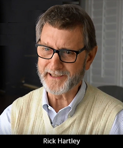
As Lawrence Romine said in his introduction, “There’s that moment when you sit in the crowd and hear Mr. Rick Hartley speak that you know you’ve arrived in PCB design.” With 50 years in the industry focused on circuit and PCB design—and as a specialist in EMI, noise, and signal integrity issues—Rick Hartley was invited to talk about PCB optimisation. But meaning what? There were a lot of things that could be optimised on a PCB.
In this particular case, Hartley was going to talk about designing boards to optimise manufacturability, with particular regard to cost-effective fabrication. I was eager to hear what he had to say, particularly having been for many years a fabricator myself, with much of my time spent talking to designers. The ones I liked best asked all the what-if questions before they began a new design. The ones who caused the most annoyance belonged to the “over-the-wall” category. It gave me enormous satisfaction to arrange for them to visit our factory then surprise them with an invitation to help manufacture what they had designed. They would say, “I never knew it was that complicated.”
Hartley made it clear that although he could easily make a really long presentation on the subject—eight hours at least—he would cover as much as he could in his conference time slot. His overarching message, which he repeated many times, was “Talk to the fabricator,” commenting, “Fabricators know their processes and know them well. If we ship them designs that make sense, that are well-thought-out, they won’t have scrap. When they have high levels of scrap, it’s because we as designers have not done our job right.” The question to ponder was, “When there’s scrap at a fab house, who do you think pays?”
He discussed some of the key items of information that a fabricator would check once a design was received for manufacture, the first of which was board size in the context of economic material utilisation. Next came the material choice, number of layers, and layers per given board thickness. There was still a common presumption that all circuit boards must be one-sixteenth of an inch (62 mils) thick, like the early single and double-sided designs and the card-guides they fitted into. He urged designers to think carefully about the consequences when nominating board thickness, commenting on the difficulty in manufacturing a 16-layer controlled impedance design to a finished thickness of 62 mils.
He recalled an early experience of working with a fabricator to optimise the finished thickness of a series of 12-layer designs, taking into account the issues of performance, ease-of-manufacture, and cost-effectiveness, arriving at a figure of 75 ±5 mils. Drilling cost obviously increased with the number of holes, but probably more significant factors were minimum hole size and aspect ratio, pad-to-hole size ratio, and power and ground plane clearance from the hole wall. IPC standards were a useful reference for clearances and tolerances.
Continuing down his list of critical parameters, he discussed minimum conductor widths and spaces, particularly in relation to copper foil thickness and copper balance layer-to-layer. Explaining at each stage the reasons for preferred and non-preferred options, he covered the topics of solder masks and component legends, final finishes, and metallisations, as well as edge connectors, controlled impedance, and design-specific features.
For guidance on actual fabrication cost, he referred to the “fabrication report card” described by Happy Holden, where each line-item was associated with a weighting factor, and low numbers were to be preferred when establishing cost per panel. Mention of cost per panel led to a discussion on preferred panel sizes and material utilisation, reminding designers that the panel also had to accommodate test coupons, tooling holes and copper-thieving in the perimeter, and room for profile-machining between individual circuits.
Again, the advice was, “Talk to the fabricators and make sure your design fits their panels and their processes.” Not forgetting the assembler, Hartley reminded designers to be aware of the keep-out areas necessary for supporting and transporting the board through the assembly process and not to fill them with components. Alternatively, put multiple small boards into a sub-panel. “Talk to the assembler as well.”Page 1 of 2
Share on:


Suggested Items
BEST Inc. Introduces StikNPeel Rework Stencil for Fast, Simple and Reliable Solder Paste Printing
06/02/2025 | BEST Inc.BEST Inc., a leader in electronic component rework services, training, and products is pleased to introduce StikNPeel™ rework stencils. This innovative product is designed for printing solder paste for placement of gull wing devices such as quad flat packs (QFPs) or bottom terminated components.
See TopLine’s Next Gen Braided Solder Column Technology at SPACE TECH EXPO 2025
05/28/2025 | TopLineAerospace and Defense applications in demanding environments have a solution now in TopLine’s Braided Solder Columns, which can withstand the rigors of deep space cold and cryogenic environments.
INEMI Interim Report: Interconnection Modeling and Simulation Results for Low-Temp Materials in First-Level Interconnect
05/30/2025 | iNEMIOne of the greatest challenges of integrating different types of silicon, memory, and other extended processing units (XPUs) in a single package is in attaching these various types of chips in a reliable way.
E-tronix Announces Upcoming Webinar with ELMOTEC: Optimizing Soldering Quality and Efficiency with Robotic Automation
05/30/2025 | E-tronixE-tronix, a Stromberg Company, is excited to host an informative webinar presented by Raphael Luchs, CEO of ELMOTEC, titled "Optimize Soldering Quality and Efficiency with Robotic Automation," taking place on Wednesday, June 4, 2025 at 12:00 PM CDT.
CE3S Launches EcoClaim Solutions to Simplify Recycling and Promote Sustainable Manufacturing
05/29/2025 | CE3SCumberland Electronics Strategic Supply Solutions (CE3S), your strategic sourcing, professional solutions and distribution partner, is proud to announce the official launch of EcoClaim™ Solutions, a comprehensive recycling program designed to make responsible disposal of materials easier, more efficient, and more accessible for manufacturers.