


 It’s Only Common Sense: If You’re Not Differentiated, You’re Dead
 Alpha Insights, Performance by Design: The Future of PCB Manufacturing in the Midwest
 Happy’s Tech Talk #43: Engineering Statistics Training With Free Software


Breakthrough Quantum-Dot Transistors Create a Flexible Alternative to Conventional Electronics
October 30, 2020 | Los Alamos National LaboratoryEstimated reading time: 2 minutes
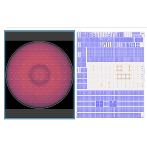
Researchers at Los Alamos National Laboratory and their collaborators from the University of California, Irvine have created fundamental electronic building blocks out of tiny structures known as quantum dots and used them to assemble functional logic circuits. The innovation promises a cheaper and manufacturing-friendly approach to complex electronic devices that can be fabricated in a chemistry laboratory via simple, solution-based techniques, and offer long-sought components for a host of innovative devices.
“Potential applications of the new approach to electronic devices based on non-toxic quantum dots include printable circuits, flexible displays, lab-on-a-chip diagnostics, wearable devices, medical testing, smart implants, and biometrics,” said Victor Klimov, a physicist specializing in semiconductor nanocrystals at Los Alamos and lead author on a paper announcing the new results in the October 19 issue of Nature Communications.
For decades, microelectronics has relied on extra-high purity silicon processed in a specially created clean-room environment. Recently, silicon-based microelectronics has been challenged by several alternative technologies that allow for fabricating complex electronic circuits outside a clean room, via inexpensive, readily accessible chemical techniques. Colloidal semiconductor nanoparticles made with chemistry methods in much less stringent environments are one such emerging technology. Due to their small size and unique properties directly controlled by quantum mechanics, these particles are dubbed quantum dots.
A colloidal quantum dot consists of a semiconductor core covered with organic molecules. As a result of this hybrid nature, they combine the advantages of well-understood traditional semiconductors with the chemical versatility of molecular systems. These properties are attractive for realizing new types of flexible electronic circuits that could be printed onto virtually any surface including plastic, paper, and even human skin. This capability could benefit numerous areas including consumer electronics, security, digital signage and medical diagnostics.
A key element of electronic circuitry is a transistor that acts as a switch of electrical current activated by applied voltage. Usually transistors come in pairs of n- and p-type devices that control flows of negative and positive electrical charges, respectively. Such pairs of complementary transistors are the cornerstone of the modern CMOS (complementary metal oxide semiconductor) technology, which enables microprocessors, memory chips, image sensors and other electronic devices.
The first quantum dot transistors were demonstrated almost two decades ago. However, integrating complementary n- and p-type devices within the same quantum dot layer remained a long-standing challenge. In addition, most of the efforts in this area have focused on nanocrystals based on lead and cadmium. These elements are highly toxic heavy metals, which greatly limits practical utility of the demonstrated devices.
The team of Los Alamos researchers and their collaborators from the University of California, Irvine have demonstrated that by using copper indium selenide (CuInSe2) quantum dots devoid of heavy metals they were able to address both the problem of toxicity and simultaneously achieve straightforward integration of n- and p-transistors in the same quantum dot layer. As a proof of practical utility of the developed approach, they created functional circuits that performed logical operations.
The innovation that Klimov and colleagues are presenting in their new paper allows them to define p- and n-type transistors by applying two different types of metal contacts (gold and indium, respectively). They completed the devices by depositing a common quantum dot layer on top of the pre-patterned contacts. “This approach permits straightforward integration of an arbitrary number of complementary p- and n-type transistors into the same quantum dot layer prepared as a continuous, un-patterned film via standard spin-coating,” said Klimov.
Share on:


Testimonial
"We’re proud to call I-Connect007 a trusted partner. Their innovative approach and industry insight made our podcast collaboration a success by connecting us with the right audience and delivering real results."
Julia McCaffrey - NCAB GroupSuggested Items
Nolan’s Notes: Tariffs, Technologies, and Optimization
10/01/2025 | Nolan Johnson -- Column: Nolan's NotesLast month, SMT007 Magazine spotlighted India, and boy, did we pick a good time to do so. Tariff and trade news involving India was breaking like a storm surge. The U.S. tariffs shifted India from one of the most favorable trade agreements to the least favorable. Electronics continue to be exempt for the time being, but lest you think that we’re free and clear because we manufacture electronics, steel and aluminum are specifically called out at the 50% tariff levels.
MacDermid Alpha & Graphic PLC Lead UK’s First Horizontal Electroless Copper Installation
09/30/2025 | MacDermid Alpha & Graphic PLCMacDermid Alpha Electronics Solutions, a leading supplier of integrated materials and chemistries to the electronics industry, is proud to support Graphic PLC, a Somacis company, with the installation of the first horizontal electroless copper metallization process in the UK.
Electrodeposited Copper Foils Market to Grow by $11.7 Billion Over 2025-2032
09/18/2025 | Globe NewswireThe global electrodeposited copper foils market is poised for dynamic growth, driven by the rising adoption in advanced electronics and renewable energy storage solutions.
MacDermid Alpha Showcases Advanced Interconnect Solutions at PCIM Asia 2025
09/18/2025 | MacDermid Alpha Electronics SolutionsMacDermid Alpha Electronic Solutions, a global leader in materials for power electronics and semiconductor assembly, will showcase its latest interconnect innovations in electronic interconnect materials at PCIM Asia 2025, held from September 24 to 26 at the Shanghai New International Expo Centre, Booth N5-E30
Trouble in Your Tank: Implementing Direct Metallization in Advanced Substrate Packaging
09/15/2025 | Michael Carano -- Column: Trouble in Your TankDirect metallization systems based on conductive graphite are gaining popularity throughout the world. The environmental and productivity gains achievable with this process are outstanding. Direct metallization reduces the costs of compliance, waste treatment, and legal issues related to chemical exposure. A graphite-based direct plate system has been devised to address these needs.