-
- News
- Books
Featured Books
- pcb007 Magazine
Latest Issues
Current IssueSales: From Pitch to PO
From the first cold call to finally receiving that first purchase order, the July PCB007 Magazine breaks down some critical parts of the sales stack. To up your sales game, read on!
The Hole Truth: Via Integrity in an HDI World
From the drilled hole to registration across multiple sequential lamination cycles, to the quality of your copper plating, via reliability in an HDI world is becoming an ever-greater challenge. This month we look at “The Hole Truth,” from creating the “perfect” via to how you can assure via quality and reliability, the first time, every time.
In Pursuit of Perfection: Defect Reduction
For bare PCB board fabrication, defect reduction is a critical aspect of a company's bottom line profitability. In this issue, we examine how imaging, etching, and plating processes can provide information and insight into reducing defects and increasing yields.
- Articles
- Columns
- Links
- Media kit
||| MENU - pcb007 Magazine
Polar, Anritsu Team for Production Testing of PCB Insertion Loss
January 26, 2021 | Polar InstrumentsEstimated reading time: 1 minute

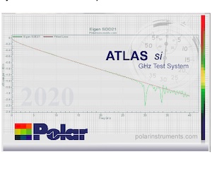
Polar Instruments and Anritsu Corporation have introduced a solution for the production testing of PCB insertion loss. Atlas vector network analysers (VNAs) are especially focused on material qualification and testing high-speed serial data busses at the PCB fabrication level. This combines the industry standard Atlas insertion loss test and data logging software with the Anritsu MS46524B-043 43.5 GHz VNA. The combination of industry standard Atlas test environment with Anritsu’s renowned ShockLine Vector Network Analyser technology delivers new standards in accuracy and ease of use when production testing PCBs for insertion loss at the fabrication level.
“Combining the Polar Atlas test software environment with the unprecedented value of the Anritsu ShockLine VNA brings 43GHz insertion loss testing within reach of leading PCB fabricators,” explains Terence Chew, Managing Director of Greater China operations of Polar Asia Pacific. “One of the key strengths linking Polar Atlas software with the ShockLine VNA is the delivery of a familiar measurement environment for fabricators accustomed to the Polar CITS and Atlas user interface for the test of high speed PCB characteristics during and immediately post fabrication.”
“Our collaboration will leverage the advanced technologies of the ShockLine VNAs with Polar Instruments’ measurement software to develop an efficient VNA-based solution that addresses current and future Delta-L test needs for emerging PCB designs,” said Stan Oda, Anritsu ShockLine VNA Product Manager.
Atlas is part of a suite of signal integrity measurement, documentation and modeling tools from Polar, enabling OEM PCB specifiers and fabricators to accurately communicate PCB signal integrity requirements across the supply chain. From tools for designing and communicating layer stackup through to tools for both modeling and measuring characteristic impedance and insertion loss. Atlas for Anritsu VNA helps close the loop with the metrology side of the equation for ultra high speed signaling applications whilst Si9000e and Speedstack Si provide modeling and documentation to ensure that PCBs are produced with the highest possible yields from a high speed perspective.
For further information please contact your local Polar office, contact details maybe found at polarinstruments.com.
Suggested Items
TRI to Exhibit at SMTA Queretaro Expo 2025
07/16/2025 | TRITest Research, Inc. (TRI), the leading provider of test and inspection systems for the electronics manufacturing industry, is pleased to announce plans to exhibit at the SMTA Querétaro Expo 2025, scheduled to take place on July 24, 2025, at the Querétaro Centro de Congresos y Teatro Metropolitano.
Knocking Down the Bone Pile: Addressing End-of-life Component Solderability Issues, Part 4
07/16/2025 | Nash Bell -- Column: Knocking Down the Bone PileIn 1983, the Department of Defense identified that over 40% of military electronic system failures in the field were electrical, with approximately 50% attributed to poor solder connections. Investigations revealed that plated finishes, typically nickel or tin, were porous and non-intermetallic.
Meet the Author Podcast: Martyn Gaudion Unpacks the Secrets of High-Speed PCB Design
07/16/2025 | I-Connect007In this special Meet the Author episode of the On the Line with… podcast, Nolan Johnson sits down with Martyn Gaudion, signal integrity expert, managing director of Polar Instruments, and three-time author in I-Connect007’s popular The Printed Circuit Designer’s Guide to... series.
TTCI Joins Printed Circuit Engineering Association to Strengthen Design-to-Test Collaboration and Workforce Development
07/09/2025 | The Test Connection Inc.The Test Connection Inc. (TTCI), a leading provider of electronic test and manufacturing solutions, is proud to announce its membership in the Printed Circuit Engineering Association (PCEA), further expanding the company’s efforts to support cross-functional collaboration, industry standards, and technical education in the printed circuit design and manufacturing community.
Study on Resonance Mitigation in Metallic Shielding for Integrated Circuits
07/08/2025 | Maria Cuesta-Martin, Victor Martinez, Vidal Gonzalez Aguado, Würth ElektronikInherent cavity resonant modes often lead to significant degradation of shielding effectiveness, responsible for unwanted electromagnetic coupling. Cavity resonant modes of the metal shielding enclosure can produce two adverse problems: the mutual coupling among different RF modules and shielding effectiveness reduction of the metal enclosure. The cabinets serve to shield certain components from electromagnetic interference (EMI). However, these cavities present some resonance peaks at 5 GHz, making it impossible to use them at higher frequencies.