


 The Government Circuit: New Council Now Helps Shape Policy Decisions in the Electronics Supply Chain
 Learning With Leo: Soldering—The Interpretation Problem
 Nolan’s Notes: The ROI of Setup Optimization


CyberOptics Corporation, a leading global developer and manufacturer of high-precision 3D sensing technology solutions, will present a technical paper at PhotoMask Japan on April 20th at 6 p.m. CDT / April 21st at 8 a.m. JST.
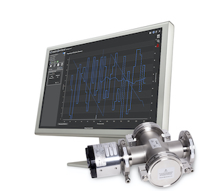
Vidya Vijay, Senior Program Manager, CyberOptics, will present the technical paper titled ‘Improving Yields and Tool Uptime with the In-Line Particle Sensor™ in Semiconductor Environments.’
Minimizing particles in semiconductor fab environments remains a critical success factor. Stringent manufacturing requirements and a focus on maximizing yields and tool uptimes drives a need for best-in-class practices for a contamination-free process environment. Quickly identifying when and where airborne particles originate, as well as the source of the contamination, proves challenging.
To address this critical need, an In-Line Particle Sensor™ (IPS™) can be used for effective semiconductor tool set-up and process diagnostics. The device and accompanying CyberSpectrum™ software can identify, measure, monitor and troubleshoot particles down to 0.1µm in gas and vacuum lines 24/7/365 in semiconductor process equipment.
The IPS is an extension of the industry-leading WaferSense® and ReticleSense® Airborne Particle Sensors (APS™ and APSRQ™) that are documented by fabs as the Best-Known Method (BKM). Combined with CyberSpectrum software, it is particularly relevant for EUVL tools where the ability to monitor particles in-line can significantly improve EUVL tool yield and productivity. For example, it can be installed at the vacuum line in between the EUV process chamber and the vacuum pump, saving significant time compared to current methods of sending a monitor dummy reticle into the EUV system to check for particles before and after sending the reticle into the EUVL. The IPS is always on and collecting particle data, which is especially critical during chamber purging.
Process and equipment engineers can speed up equipment qualification with real-time, 24/7 monitoring, compare past and present data, as well as one tool to another. Contamination sources can be identified quickly and the effects of cleaning, adjustments and repairs can be seen in real-time. Fabs can shorten equipment maintenance cycles, lower equipment expenses and optimize preventative maintenance plans. Overall, by adopting the IPS solution, fabs can recognize significant reductions in time and expense while improving yields and productivity.
About CyberOptics
CyberOptics Corporation is a leading global developer and manufacturer of high-precision 3D sensing technology solutions. CyberOptics’ sensors are used for inspection and metrology in the SMT and semiconductor markets to significantly improve yields and productivity. By leveraging its leading edge technologies, the Company has strategically established itself as a global leader in high precision 3D sensors, allowing CyberOptics to further increase its penetration of key vertical markets. Headquartered in Minneapolis, Minnesota, CyberOptics conducts worldwide operations through its facilities in North America, Asia and Europe. For more information, visit www.cyberoptics.com.


