


 Global Sourcing Spotlight: Making Global Sourcing Simple Again
 The Government Circuit: New Council Now Helps Shape Policy Decisions in the Electronics Supply Chain
 Learning With Leo: Soldering—The Interpretation Problem


At the 30th anniversary of NEPCON China, Koh Young Technology, the industry leader in True3D measurement-based inspection solutions will exhibit a full suite of inspection and process control solutions at NEPCON China in Booth 1H15 Zone A on April 21-23, 2021 at the Shanghai World Expo Exhibition & Convention Centre.
During the exhibition, Koh Young will exhibition eight products that solve electronics assembly challenges:
- Automated Solder Paste Dispensing: The KY8030-3 automatically dispenses paste with its Auto-Rework option. The high-precision and user-friendly dispensing system eliminates costly mistakes due to insufficient solder causing open joints, lean fillets, and weak joints.
- Review 3.0: Provides intuitive review and verification station.
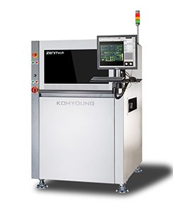
- FPCB Substrate Handling: The Zenith F is the ideal solution for high-volume FPCB inspection. Due to the thinner and pliable nature of the flexible printed circuit boards, special handling with dedicated expertise is required in comparison to traditional printed circuit boards.
- Hotbar Inspection: The Zenith F is the industry’s only solution to base its inspection criteria on the IPC-610 standards using True 3D inspection performance for hotbar soldering.
- KAP (Koh Young Auto Programming): The innovative geometry-based KAP software solution reduces the programming process to minimize time to production and reduces costs.
- Whole-board Foreign Material Inspection (WFMI): Inspection goes beyond components and solder joints. The Zenith Alpha combines 2D with True 3D to identify foreign material such as burr, solder balls, chips, and other debris that may lead to costly field failures.
- Flux Inspection: Combining innovative vision algorithms and high-resolution optics for the semiconductor industries, the Meister S is a solution provider for flux inspection.
- Thin Solder Inspection: The Meister S has been qualitied for mass production by major semiconductor foundries and micro-LED companies for solder inspection down to 10um.
- Crack Inspection: The Meister D is a solution targeting die and small MLCCs using an integrated measurement tool with defect analysis software based on advanced optics and AI engines. The system inspects micro cracks, chipping, foreign material, and more.
- True 3D Profiling: Using patented technologies, the Neptune C+ is the industry’s first 3D in- line DPI and thickness measurement solution for transparent material inspection. The system allows manufacturers to explore the depths of its process and accurately find defects with 2D, 3D, and cross-section views.
- Bubble Inspection using AI-Powered Capabilities: With its proprietary machine learning technology, the Neptune C+ offers enhanced inspection capabilities enabling autonomous bubble inspection without teaching and endless tuning.
7. KY-P3: Breakthrough in 3D Automated Pin Inspection Solutions
- Versatile Handling Mechanisms: Handling products at the back-end process has proven to be a challenge, yet Koh Young provides a perfect product lineup with versatile handling mechanisms. It offers multiple board and carrier handling solutions to accommodate multiple types of PCBs, connectors, terminals, and even final assemblies with housing pins.
8. KSMART Solutions: True Smart Factory Solution
- Turn Data into Insight: AI-powered KSMART solutions help automate process control while focusing on data management, analysis, and optimization. It collects data from across the factory for defect detection, real-time optimization, enhanced decisions, and traceability to improve metrics, increase quality, and lower costs by eliminating variances, false calls, and escapes.
- Convert data into knowledge for effective and quality-driven actions
- Deliver an AI-powered process analysis and optimization tool
- Achieve an autonomous process optimization facility
To learn more about these award-winning technologies from Koh Young, register for NEPCON China. If you cannot attend the exhibition, you can still learn more about our celebrated solutions at it at www.kohyoung.com.
Be sure to visit I-007eBooks to download a copy of Koh Young's micro eBook 'The Printed Circuit Assembler's Guide to...SMT Inspection' today!
About Koh Young
Established in 2002, Koh Young pioneered the market by launching the first 3D Solder Paste Inspection (SPI) system using a patented dual-projection Moiré technology. Since then, it has become the global leader in 3D measurement-based SPI and Automated Optical Inspection (AOI) equipment for the electronics industry. Based on its True3D™ measurement-based inspection technology, Koh Young has developed new solutions for challenges with Machining Optical Inspection (MOI), Dispensing Process Inspection (DPI), and Semiconductor Packaging Inspection (MEISTER Series), as well as branching out to Medical Robotics for brain surgery (KYMERO). Through its technological innovations, Koh Young has secured thousands of global customers, and maintains the largest global market share in the SPI and AOI markets. Additionally, by adopting its user-centric R&D activities, it continues to leverage core competencies and develop innovative solutions for new and existing markets. Its activities stem from the corporate headquarters in Korea to its sales and support offices in Germany, Japan, Singapore, Vietnam, Penang, China, Brazil, Argentina, Canada, Mexico, and the United States. These local facilities ensure it keeps in close contact with the market, and more importantly, its growing customer base to provide access to an award-winning network of inspection and measurement experts. Learn why so many electronics manufacturers trust Koh Young for reliable inspection at kohyoung.com.


