


 The Marketing Minute: If Your Marketing Budget Gets Cut in Half, Then What?
 Punching Out: How Are the Big Boys in Electronics Doing?
 It’s Only Common Sense: Complexity Is the Enemy of Profit


Novel Beamforming Network Solution for Single Layer Printed Circuit Board Implementation
October 7, 2021 | Tokyo Institute of TechnologyEstimated reading time: 2 minutes
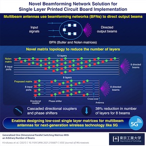
Wireless technology is responsible for enabling pivotal innovations such as radio and satellite communication. Central to these systems are antennas that can transmit and receive signals. As the scope of wireless technology continues to grow, the next generation of wireless systems requires multibeam antennas that are capable of efficiently handling multiple beams. To maintain stable and reliable connections between transmitters and receivers, these multibeam antennas use beamforming networks (BFNs) like the Butler and Nolen matrices. These BFNs control and direct output signals using a combination of electrical components including phase shifters and directional couplers. The type of BFNs used determines the structure of the circuit and the number of layers the circuit would need to generate a certain number of beams.
BFNs have become even more necessary for implementing 5G technology in the millimeter-wave range as these waves are much more prone to interference. This has led researchers to look into BFNs and improve them to provide low cost-solutions for single-layer printed circuit board (PCB) implementation. In other words, the goal is to produce a configuration with the maximum number of beams and the lowest number of layers.
Now in a study published in IEEE Journal of Microwaves, scientists from Tokyo Tech, Japan, and the European Space Agency, The Netherlands, have introduced a novel one-dimensional switching matrix that achieves a reduction in the number of layers when compared to conventional matrices. Elaborating their approach, Prof. Jiro Hirokawa from Tokyo Tech explains, "We have numerically found the parameters of the directional couplers (including crossovers) and phase shifters that determine the structure of the circuit for an arbitrary number of beams in the generalized configuration of the orthogonal matrix forming multiple antenna beams. The discovery improves over previously known solutions addressing the specific challenges of planar implementation."
The novel matrix topology overcomes the limitations of conventional beamforming matrices. While Butler matrices are limited in the number of beams they can generate to integer powers of two, the proposed solution can generate an arbitrary number of beams. Unlike Nolen matrices, an even distribution of the signals between the phase shifters and directional couplers is possible, resulting in more uniform output signals.
Compared to the conventional Butler and Nolen matrices, the novel matrix topology also achieves a reduction in the number of layers when the number of beams is five and above, reaching a reduction ratio of 38% with 8 beams. "This reduction ratio is very useful for passive antenna orthogonal beamforming matrices. It is expected to benefit the design of next-generation wireless mobile systems and satellite communication microwave payloads," explains Prof. Hirokawa.
The various improvements to the output signal and the compaction in the number of layers allows the proposed BFN to be implemented in low-cost printed circuit boards, making the manufacture of multibeam antennas for the next-generation wireless systems viable and cost-effective.
Read the original article, here.
Share on:


Testimonial
"Advertising in PCB007 Magazine has been a great way to showcase our bare board testers to the right audience. The I-Connect007 team makes the process smooth and professional. We’re proud to be featured in such a trusted publication."
Klaus Koziol - atgSuggested Items
TPCA Launches AI-Powered PCB GPT Knowledge Platform
05/15/2026 | TPCAThe Taiwan Printed Circuit Association (TPCA) has launched the "PCB GPT Industry Knowledge Platform," which uses generative AI to connect PCB professional knowledge services and help the industry improve the efficiency of cross-border and professional talent training.
Heilind Electronics Expands Circuit Protection Portfolio with OptiFuse Partnership
05/15/2026 | Globe NewswireHeilind Electronics, a leading global distributor of interconnect, electromechanical, and industrial automation products, is pleased to announce a new supplier partnership with OptiFuse, a manufacturer of overcurrent and circuit protection devices serving a broad range of industrial and electronic applications.
New Book Explores How UV Technology Is Transforming Electronics Protection, Efficiency, and Sustainability
05/14/2026 | I-Connect007I-Connect007 proudly announces the recent release of The Printed Circuit Designer’s Guide to…™ UV Curable Conformal Coatings. Authored by respected industry technologists Brian Chislea and Cody Schoener, PhD, of Dow, Inc., this new volume offers a comprehensive exploration of UV-curable conformal coatings and their expanding role in improving the protection, performance, and sustainability of electronic assemblies.
STARTEAM GLOBAL Achieves A Score in CDP’s Supplier Engagement Assessment
05/14/2026 | STARTEAM GLOBALSTARTEAM GLOBAL has achieved an A score in CDP’s Supplier Engagement Assessment (SEA).
Zhen Ding Reports Record 1Q26 Revenue; Up 1.6% YoY
05/14/2026 | Zhen Ding TechnologyZhen Ding Technology Holding Limited, a global leading PCB manufacturer, announced its consolidated financial results for the first quarter of 2026. First quarter revenue reached NT$40,728 million, up 1.6% YoY and setting a record high for the same period. Net income was NT$2,047 million, and net income attributable to the parent company was NT$1,426 million, with EPS of NT$1.33.