-

-
News
News Highlights
- Books
Featured Books
- smt007 Magazine
Latest Issues
Current Issue
Wire Harness Solutions
Explore what’s shaping wire harness manufacturing, and how new solutions are helping companies streamline operations and better support EMS providers. Take a closer look at what’s driving the shift.

Spotlight on Europe
As Europe’s defense priorities grow and supply chains are reassessed, industry and policymakers are pushing to rebuild regional capability. This issue explores how Europe is reshaping its electronics ecosystem for a more resilient future.

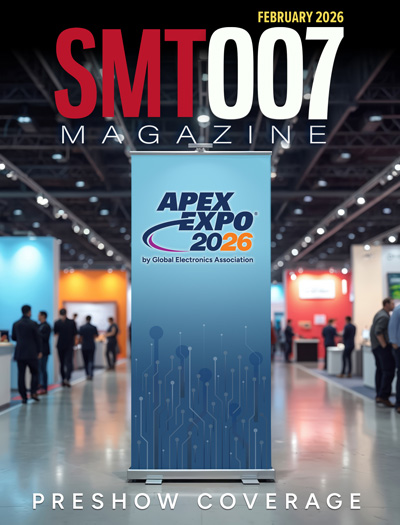
APEX EXPO 2026 Preshow
This month, we take you inside the annual trade show of the Global Electronics Association, to preview the conferences, standards, keynotes, and other special events new to the show this year.
- Articles
- Columns
- Links
- Media kit
||| MENU - smt007 Magazine
Koh Young Launches the Meister D+ for Semiconductor Package Inspection to the Americas Market
October 13, 2021 | Koh YoungEstimated reading time: 2 minutes
Koh Young, the industry leader in True3D™ measurement-based inspection solutions, announces the release of its new Meister D+ semiconductor inspection solution. Premium True3D™ Inspection Solution for Chiplets and System-in-Package (SiP) devices including die and surface mount components. The new Meister D+ is an extension of the Meister product family that features solutions ranging from solder paste, printed bumps, and solder ball to small components like 0201Ms and highly reflective die.
Meister D+: Industry Leading Inspection Systems for Advanced Packaging and Semiconductor Applications
As advanced packages continue evolving, device thickness is paramount since consumers demand smaller products with more functionality. As such, the die must be thinned, which creates a mirror-like surface that challenges optical inspection due to its highly reflective surface. Additionally, tight interspacing and increasing aspect ratios further complicate inspection. Yet, as the name implies, the Meister D+ dominants these challenges with industry leading True3D measurement accuracy and inspection technologies.
The latest Meister D+ system is perfected for component and die inspection, while delivering fast, accurate inspection from an 8-projector probe. It targets MCM/SiP/Chiplet inspection with integrated measurement and defect analysis software built on a proprietary AI engine. Beyond 0201M (008004) microchips, 10um bump height, and 5um gap spacing, it detects die defects like micro-cracks, chippings, and foreign material with high accuracy/repeatability. Additionally, this 3D solution supports a wide range of inspection capabilities: missing, offset, rotation, polarity, dimension, co-planarity, and more.
With its Moiré technology, new 12MegaPixel/5-micron optics, and 300mm^2/second inspection speed, the Meister D+ is the first solution for production-speed 3D inspection for modules combining microchips and mirror-finish die. With its user-friendly GUI and programming wizards, it virtually eliminates fine-tuning and teaching, which quickens the production ramp. Plus, its IPC-CFX-2591, IPC-HERMES-9852, and IPC-DPMX-2581 compatibility makes connectivity simple and secure.
With innovative technologies, Meister D+ delivers best-in-class performance and functionality. Its inspection capabilities have already been qualified for mass production by major semiconductor companies throughout the world. The recognized leader in electronics measurement and inspection, Koh Young continues to deliver solutions for the electronics manufacturing industry.
To learn more about our award-winning technologies from Koh Young, visit us at SMTA International in booth 3319. As the Premiere Sponsor for SMTA International, Koh Young America is excited to reconnect and collaborate in-person, while ensuring COVID safety protocols are implemented and upheld for your health and ours. You can register to attend the in-person conference and exposition at smta.org. If you cannot attend, you can still learn more about our best-in-class inspection solutions at our regional website www.kohyoungamerica.com.
Be sure to check out the free 12-part Webinar Series Converting Process Data Into Intelligence, presented by Koh Young experts Joel Scutchfield and Ivan Aduna and download Koh Young's free eBooks The Printed Circuit Assembler’s Guide to... SMT Inspection: Today, Tomorrow, and Beyond published by I-Connect007.
Testimonial
"In a year when every marketing dollar mattered, I chose to keep I-Connect007 in our 2025 plan. Their commitment to high-quality, insightful content aligns with Koh Young’s values and helps readers navigate a changing industry. "
Brent Fischthal - Koh YoungSuggested Items
SEMIEXPO Heartland 2026 Highlights Automotive Electronics and Smart Manufacturing Innovation
04/29/2026 | SEMIThe second edition of SEMIEXPO Heartland opens this week, April 29-30 at the Detroit Marriot at the Renaissance Center in Detroit, Michigan, centered around smart manufacturing, automotive electronics, and workforce development.
SEMI Europe Outlines Six Key Recommendations to Strengthen Chips Act 2.0
04/28/2026 | SEMISEMI Europe announced the publication of its Position Paper on the Chips Act 2.0, presenting a set of strategic recommendations aimed at reinforcing and future-proofing Europe’s semiconductor policy framework.
MacDermid Alpha to Debut Zero-PFAS Die Attach Paste ATROX CD 560-1 at SEMICON Southeast Asia 2026
04/27/2026 | MacDermid Alpha Electronics SolutionsMacDermid Alpha Electronics Solutions will debut ATROX® CD 560-1, a zero-PFAS conductive die attach paste, at SEMICON Southeast Asia 2026, May 5–7, in Kuala Lumpur, Booth 2423.
Indium Corporation Joins India’s IDSPS Industry Consortium Partnership
04/24/2026 | Indium CorporationIndium Corporation announced that it has joined the Indian Design, Semiconductor, Packaging and Systems (IDSPS) program, a national initiative supporting R&D, workforce development, and global supply-chain growth.
SEMICON Southeast Asia 2026 to Convene Leaders in Malaysia for Semiconductor Growth
04/22/2026 | SEMISEMICON Southeast Asia (SEMICON SEA) 2026, the region’s premier platform for the global semiconductor and electronics manufacturing supply chain, will return to the Malaysia International Trade and Exhibition Centre (MITEC) in Kuala Lumpur from 5 to 7 May. Registration is open.


