


 Defense Speak Interpreted: JADC2—Why It’s More Relevant Than Ever in Drone Warfare
 Beyond the Board: Orbital High Ground—Why Space Superiority Is Slipping Away
 The Government Circuit: Trump’s Trade War Disrupts the Electronics Ecosystem


AT&S Starts Construction of First High-tech Manufacturing Facility in Southeast Asia
October 29, 2021 | AT&SEstimated reading time: 2 minutes
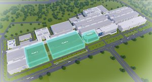
AT&S, one of the globally leading manufacturers of high-end printed circuit boards and IC substrates, headquartered in Austria (Europe), announced detailed project information on the company’s planned investment in a state-of-the-art factory for IC substrates at the Kulim Hi-Tech Park, Kedah.
During a press conference, AT&S CEO Andreas Gerstenmayer and AT&S COO Ingolf Schroeder gave insights into the planned investment, the project scope, technology details, as well as the planned activities to hire approx. 6,000 highly qualified employees.
AT&S’ new campus for the production of IC substrates in Kulim Hi-Tech Park, Kedah, involves a proposed total investment for phase 1 of RM 8.5 billion (€1.7 billion). The construction of the facility is going to start with an official groundbreaking ceremony on October 30, 2021, with commercial operations targeted to come on stream in 2024.
“I want to thank the Malaysian government as well as the MIDA (the government’s principal promotion agency under the Ministry of International Trade and Industry) for the great support throughout the entire process, from the start of our location scouting until today,” says AT&S CEO Andreas Gerstenmayer. “Already today, Malaysia is an important hub for the chip supply chain. We are convinced that Malaysia can further strengthen its position as a technology country and will develop its position in the region as a high-tech manufacturing hub in Asia,” Gerstenmayer says.
Not only will thousands of new jobs be created in the region, but Malaysia will make a name for itself as a hotspot for a completely new, first-of-its-kind technology segment. “AT&S brings the latest generation of high-end technologies to Malaysia and will establish a completely new technology sector in one of the future global microelectronic hotspots. In addition to manufacturing high-tech products, extensive R&D activities will also be conducted at this new site,” AT&S COO Ingolf Schroeder says.
All these activities require a high amount of highly qualified human resources and will boost the region’s labor market. The search profiles for employees at the new AT&S plant range from specialists, managers, and leaders in the areas of electronic, mechanical, and chemical engineers, and business. At the same time, AT&S is also looking for about 4,500 blue-collar workers who can work in a highly sophisticated shop floor environment.
Besides manufacturing, R&D will also be a focus at the new AT&S facility in Kulim. Therefore, AT&S is investigating cooperation and partnerships with leading universities in Malaysia. “These partnerships will not only help us to discover new paths for the microelectronics industry,” Andreas Gerstenmayer says. “They will also make an important contribution to the development of extensive know-how in the various areas of the microelectronics industry for Malaysia and, at the end of the day, contribute to the positive development of the society.”
Share on:


Testimonial
"In a year when every marketing dollar mattered, I chose to keep I-Connect007 in our 2025 plan. Their commitment to high-quality, insightful content aligns with Koh Young’s values and helps readers navigate a changing industry. "
Brent Fischthal - Koh YoungSuggested Items
Atg Launches Latest Large Format Test System, A9XL, with 8 Heads and 48” x 26” Panel Capability
08/01/2025 | atg Luther & Maelzer GmbHatg Luther & Maelzer GmbH (a Mycronic company) is proud to roll out a new large format test system generation based on the latest high speed atg A9 (board size up to 24” x 21”) and A9L platform.
Advint and Sayron Bring Advanced Rectifier Solutions to High-Reliability PCB Manufacturers
08/01/2025 | Advint IncorporatedAdvint Incorporated has partnered with Sayron, a leading global rectifier manufacturer, to supply cutting-edge IGBT-based DC rectifiers to high-performance PCB manufacturers across North America and beyond. Sayron’s precision-engineered rectifiers align with the stringent requirements of advanced PCB processes.
Setting Design Constraints Effectively
07/31/2025 | Stephen V. Chavez, Siemens EDAPCB design requires controlling energy within the medium of a PCB. The manner in which we control the chaos of energy is by implementing and utilizing physical and electrical rules, known as constraints, along with a specific structure and material(s) that make up what is known as the foundation of the design. These rules govern everything within the PCB structure and generally fall into two camps: performance and manufacturability. Setting this foundation correctly is extremely important and the key to success.
Direct Metallization: A Sustainable Shift in PCB Fabrication
07/31/2025 | Jim Watkowski, Harry Yang, and Mark Edwards, MacDermid Alpha Electronics SolutionsThe global electronics industry is undergoing a significant transformation, driven by the need for more resilient supply chains and environmentally sustainable manufacturing practices. Printed circuit boards (PCBs), the backbone of interconnection for electronic devices, are at the center of this shift. Traditionally, PCB fabrication has relied heavily on electroless copper, a process that, while effective, is resource-intensive and environmentally hazardous. In response, many manufacturers are turning to direct metallization technologies as a cleaner, more efficient alternative.
MacDermid Alpha Electronics Solutions Unveils Unified Global Website to Deepen Customer, Talent, and Stakeholder Engagement
07/31/2025 | MacDermid Alpha Electronics SolutionsMacDermid Alpha Electronics Solutions, the electronics business of Elements Solutions Inc, today launched macdermidalpha.com - a unified global website built to deepen digital engagement. The launch marks a significant milestone in the business’ ongoing commitment to delivering more meaningful, interactive, and impactful experiences for its customers, talent, and stakeholders worldwide.