


 The Marketing Minute: If Your Marketing Budget Gets Cut in Half, Then What?
 Punching Out: How Are the Big Boys in Electronics Doing?
 It’s Only Common Sense: Complexity Is the Enemy of Profit


Nano Dimension Sells Two DragonFly IV 3D-AME Systems to Defense and Government Agencies
December 6, 2021 | Nano Dimension Ltd.Estimated reading time: 2 minutes
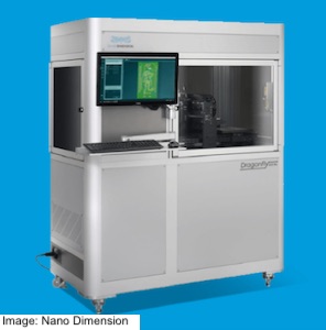
Nano Dimension Ltd., an industry-leader in Additively Manufactured Electronics (AME), Printed Electronics (PE), and Micro Additive Manufacturing (Micro-AM), announced that it has sold the first two DragonFly IV 3D-AME Printers, in addition to the two machines that have completed beta sites processes with other leading customers.
Nano Dimension is the leading provider of intelligent machines for the fabrication of AME. The new DragonFly IV system, combined with FLIGHT software, delivers new levels of quality, efficiency, and print resolution in the 3D printed electronics sector, providing increased flexibility to design any 3D geometry and create innovative new products.
DragonFly IV is a Dielectric and Conductive-Materials Additive Manufacturing System aimed for fabrication of High-Performance Electronic Devices (Hi-PEDs®) by depositing the proprietary materials simultaneously, while concurrently integrating in-situ capacitors, antennas, coils, transformers, and electro-mechanical components.
DragonFly IV 3D-AME Printer
DragonFly IV delivers improved accuracy of traces, spacing, and vias, improved PCB product quality, and the ability to design and produce 3D Hi-PEDs® in a one-step production process.
New capabilities include:
- Integration with Nano Dimension’s new FLIGHT software
- Integration of 3D elements in PCB
- 3D designed Hi-PEDs®
- Support of HDI level elements
- 75µm traces; 100µm spacing; 150µm via
- Enhanced print quality, optimizing yield with predictable conductivity
- Low thickness variation
FLIGHT Software Package
Nano Dimension’s new FLIGHT software suite provides a comprehensive first-of-a-kind ability to incorporate ECAD designs into real 3D MCAD designs, as well as intelligent verification, slicing, and job control solutions. FLIGHT enables the 3D design of electrical and mechanical features in 3-dimensions while ensuring that the new product designs comply with the system’s requirements and can then proceed directly to fabrication on the DragonFly IV.
The Flight Software Suite consists of 3 components:
1-FLIGHT Plan: Allows designers to develop viable 3D AME using both existing 2D design data, and novel 3D data. Tests show that this reduces the 3D AME design time by up to 10 times.
- Integrates 3D MCAD and ECAD capabilities for 3D Electro-Mechanical design
- Imports existing designs from major ECAD systems
- Enables the use of customers’ existing design tools
2-FLIGHT Check: This application enables design rule checks so that the designs meet the DragonFly IV requirements and are ready for printing.
- Unifies design rules for ECAD that meet the constraints of DragonFly IV
- Reduces design iteration cycles
3-FLIGHT Control: Delivers an entirely new pre-production solution that enables concurrent fabrication of both 2D and 3D multi-material Hi- PEDs®, improving productivity.
- Integrates system and job management toolsets
- Supports new file formats (STL & ODB++)
- Improves user experience through better rendering accuracy and user interface
Share on:


Testimonial
"We’re proud to call I-Connect007 a trusted partner. Their innovative approach and industry insight made our podcast collaboration a success by connecting us with the right audience and delivering real results."
Julia McCaffrey - NCAB GroupSuggested Items
New Book Explores How UV Technology Is Transforming Electronics Protection, Efficiency, and Sustainability
05/14/2026 | I-Connect007I-Connect007 proudly announces the recent release of The Printed Circuit Designer’s Guide to…™ UV Curable Conformal Coatings. Authored by respected industry technologists Brian Chislea and Cody Schoener, PhD, of Dow, Inc., this new volume offers a comprehensive exploration of UV-curable conformal coatings and their expanding role in improving the protection, performance, and sustainability of electronic assemblies.
Siemens Expands EDA Software Access Through EuroCDP Project
05/14/2026 | SiemensSiemens has become the first software provider to sign a strategic framework agreement with the European Chips Joint Undertaking (Chips JU) which aims to bolster Europe's semiconductor industry by fostering collaboration between the EU, member states and the private sector, through the European Chips Design Platform (EuroCDP) project.
Rethinking Stackup, Materials, and Tolerances in Modern Designs
05/14/2026 | Kristin Moyer, Global Electronics AssociationThe simple rectangular rigid PCB is becoming increasingly infrequent. This reality necessitates designing with concepts well outside traditional rigid PCB methodologies. For example, the designer of wearable electronics may need to implement conductive fibers integrated into the textile material. Heads-up displays, like those in VR/AR headsets and glasses, require transparent circuitry etched into the display glass. The process of designing without a rule book usually starts with something other than the traditional board design process.
New Courses: Advance Your Electronics Expertise in June and July
05/14/2026 | Global Electronics AssociationStay current with design, manufacturing, and quality standards by enrolling in one of these online instructor-led courses starting in June and July from ElectronicsU at the Global Electronics Association, designed to help professionals at every level sharpen their skills and advance their careers. These live, expert-led sessions combine flexibility with real-time interaction, allowing participants to learn directly from seasoned industry professionals while collaborating with peers worldwide. Access to all applicable IPC standards is included in the courses.
Road to Reliability: Engineering High Uptime EV Charging Infrastructure
05/13/2026 | Stanton Rak, SF Rak CompanyThe transition to EVs is no longer constrained solely by vehicle capability. Instead, it is increasingly defined by a simpler, but more unforgiving question: Will the charger work when I arrive? This high uptime does not happen by accident. As EV technology has matured, limitations in battery range, power electronics, and thermal management are no longer the primary barriers to adoption.