


 The Marketing Minute: If Your Marketing Budget Gets Cut in Half, Then What?
 Punching Out: How Are the Big Boys in Electronics Doing?
 It’s Only Common Sense: Complexity Is the Enemy of Profit


AT&S Plant in Korea is Shaping the Future of Medical Technology
December 22, 2021 | AT&SEstimated reading time: 2 minutes
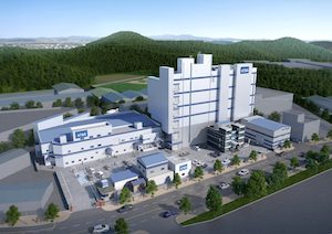
To supply the medical sector with the most modern technology in the future, AT&S has implemented a comprehensive technology upgrade at the Ansan site in Korea, with which the production technologies in the plant have been raised to a new level. “After this upgrade, around 8,000 square meters of additional production space will be available, most of which will be used for the manufacture of interconnection solutions for medical technology applications. At the same time, our production equipment was also brought up to date”, explains Christian Fleck, COO of the Automotive, Industrial and Medical business unit at AT&S.
A technological revolution is taking place in medical technology. Hearing aids, insulin pumps, and implants are already important tools for doctors today. Future applications – for example, artificial hearts, implants for specific pain suppression, or new generations of arm or leg prostheses that optimally support the natural sequence of movements, will further increase the demands on technology in medicine. Just like in other high-tech industries, products are becoming increasingly complex and multi-layered: a diagnostic device that contains two sensor functions today will need five tomorrow. The technology is becoming increasingly powerful but still has to find space in the smallest of spaces and process an increasing amount of data. This trend will increase further through new technological approaches. In diagnostics, for example, artificial intelligence will increasingly be used for data evaluation in the future, which requires the integration of new, specialized components. Circuit boards, substrates, and interconnection solutions from AT&S create the necessary platform for such highly integrated, miniaturized electronic systems.
With the newly installed systems, such as multilayer flex presses, machines for e-copper coating, and highly innovative UV lasers, production capacities will be increased by more than a quarter. On the other hand, the new infrastructure makes a significant contribution to more efficient and resource-saving circuit board production, for example in the area of??water treatment.
“The medical technology sector is an important part of the AT&S strategy and an exciting business area that we are constantly developing,” says AT&S CEO Andreas Gerstenmayer. “With our interconnection solutions, we are among the world market leaders in this segment and are already thinking intensively with our partners about solutions with which diagnostics and therapy can be revolutionized in a few years.”
The AT&S plant in Ansan specializes in the production of high-tech printed circuit boards for a wide variety of medical areas. For example, interconnection solutions for hearing aids with special sensors for targeted noise suppression in certain situations or circuit boards for cardiac catheters that enable 3D interior images of the human heart are produced. Some manufacturers also rely on AT&S technology for smart drug pumps that can automatically dispense controlled quantities of a substance when required.
Share on:


Testimonial
"Our marketing partnership with I-Connect007 is already delivering. Just a day after our press release went live, we received a direct inquiry about our updated products!"
Rachael Temple - AlltematedSuggested Items
I-Connect007 Releases The Printed Circuit Designer’s Guide to… Direct Metallization: A Guide to Complex PCB Fabrication
05/13/2026 | I-Connect007As PCB complexity continues to accelerate, fabricators and OEMs are reevaluating long-standing manufacturing processes to meet the demands of AI, HDI, advanced packaging, and next-generation electronics. To address these evolving challenges, I-Connect007 is proud to announce the release of The Printed Circuit Designer’s Guide to… Direct Metallization: A Guide to Complex PCB Fabrication, authored by MacDermid Alpha Solution’s Carmichael Gugliotti.
Driving Innovation: Selecting the Right Laser Source
04/28/2026 | Simon Khesin -- Column: Driving InnovationWhen I first joined Schmoll Maschinen, I brought experience from almost every PCB process, except for laser. As I immersed myself in laser processing, I realized why it can seem so daunting to a newcomer. The complexity arises from three intersecting factors: A vast variety of laser sources: CO2, UV-nano, green-pico, UV-pico, IR-pico, and others; a diverse range of applications: Drilling, cutting, ablation, and more; and an extensive list of materials: These have vastly different absorption rates. Choosing the right machine or laser source is rarely trivial. Even for experienced engineers, answering "Which source is best?" requires examining the business's specific goals.
Institute of Circuit Technology Spring Seminar 2026: A Bright Future in Europe
04/23/2026 | Pete Starkey, I-Connect007Through the leafy lanes and spring flowers of Warwickshire and back to Meridan, the traditional centre of England, and now officially part of the Metropolitan Borough of Solihull in the county of the West Midlands, I attended the Annual General Meeting and Spring Seminar of the Institute of Circuit Technology (ICT) on April 14. Out of the AGM came notable changes in leadership at the top of the Institute: the retirement of Mat Beadel as chair and Emma Hudson as technical director. Effective May 1, Steve Driver is the new chair, and Alun Morgan is the new technical director.
ACCM Unveils Negative and Near-zero CTE Materials for Large-Format AI Chips
04/21/2026 | Advanced Chip and Circuit MaterialsAdvanced Chip and Circuit Materials, Inc. (ACCM) has launched two new materials: Celeritas HM50, with a negative coefficient of thermal expansion (CTE) of -8 ppm/°C to offset the positive CTE and expansion of copper with temperature on circuit boards, and Celeritas HM001, with near-zero CTE and the low-loss performance needed for high-speed signal layers to 224 Gb/s and faster in artificial intelligence (AI) circuits.
Fresh PCB Concepts: Designing PCBs for Harsh Environments—Reliability Is Engineered Upstream
04/23/2026 | Team NCAB -- Column: Fresh PCB ConceptsWhen engineers hear the phrase “harsh environment,” they usually think of the extreme temperature swings, vibration and shock, pressure changes, or radiation in aerospace. However, aerospace is not the only harsh environment where electronic assemblies must survive. Automotive power electronics, downhole oil and gas tools, marine controls, rail systems, defense platforms, and industrial automation equipment all expose PCBs to environments that are equally unforgiving. The stress mechanisms may differ, but the physics does not.