


 Global Sourcing Spotlight: Making Global Sourcing Simple Again
 The Government Circuit: New Council Now Helps Shape Policy Decisions in the Electronics Supply Chain
 Learning With Leo: Soldering—The Interpretation Problem


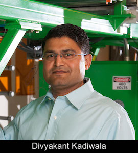
Averatek is pleased to announce that VP of Manufacturing Divyakant Kadiwala will present the paper entitled, “Surface Treatment for Soldering Aluminum PCBs to Conventional Copper PCBs” during the IPC APEX EXPO Technical Conference, scheduled to take place Jan. 22-27, 2022 at the San Diego Convention Center in California. The paper was co-authored by Nazarali Merchant, Ph.D., Senior Materials Scientist for Averatek.
Soldering is the preferred method for mounting SMDs and connecting circuit boards. But that brings in processing challenges. Soldering to aluminum requires an additional surface treatment or the use of conductive epoxy. These are cost-prohibitive and have reliability challenges and existing products like solders, fluxes, tack agents, cleaners etc. are formulated for Cu-PCBs and do not work on aluminum.
An advanced surface treatment technology will be presented that addresses all these constraints. Once printed on aluminum using conventional printing techniques such as screen, stencil etc., it is cured thermally in a convection oven at low temperatures, leaving a non-conductive deposit on the pads. This is followed by conventional process i.e. print solder over the treated pads, place components and then reflow resulting in finished Al-PCBs. It can also be used to solder Al-PCBs to flexible and rigid Cu-PCBs.
This is a paradigm shift in the industry which opens up many new applications, including those in the RFID, LED, and automotive industries. We will show solder cross-sections and shear data on the soldered joints, including Al-PET to Cu-PCB, Al-PET to Cu-Polyimide using aluminum metallization with low temperature Bi-Sn-Ag solders.
Kadiwala is a process development and project management leader in developing innovative products from laboratory concepts to large-scale manufacturing. He has 15+ years of multi-national experience with utilizing emerging technologies in strategic roles.
Kadiwala holds a BS in Chemical Engineering from the University of Mumbai, and a Master’s degree in Manufacturing Systems Engineering from the University of Wisconsin.
Merchant has 20 years of successful deliverables in PCBs, semiconductor packaging, metallurgy, welding consumables and processes, superconductors, fuel cells, batteries, solar cells, and failure analysis. His work has resulted in six US patents, three US patent applications under review, and 25 technical publications.
Merchant holds Doctorate and Master’s degree in Materials Engineering from the University of Illinois, and a Bachelor of Technology in Metallurgical Engineering from IIT of Bombay.
About Averatek
Averatek is a technology innovation company that develops and manufactures key chemistries, and licenses their associated advanced processes, for: very high-density printed circuit boards, semiconductor packaging, RF and millimeter-wave passive components, simplified assembly to aluminum. For more information, visit www.averatek.com.


