-
-
News
News Highlights
- Books
Featured Books
- pcb007 Magazine
Latest Issues
Current IssueThe Hole Truth: Via Integrity in an HDI World
From the drilled hole to registration across multiple sequential lamination cycles, to the quality of your copper plating, via reliability in an HDI world is becoming an ever-greater challenge. This month we look at “The Hole Truth,” from creating the “perfect” via to how you can assure via quality and reliability, the first time, every time.
In Pursuit of Perfection: Defect Reduction
For bare PCB board fabrication, defect reduction is a critical aspect of a company's bottom line profitability. In this issue, we examine how imaging, etching, and plating processes can provide information and insight into reducing defects and increasing yields.
Voices of the Industry
We take the pulse of the PCB industry by sharing insights from leading fabricators and suppliers in this month's issue. We've gathered their thoughts on the new U.S. administration, spending, the war in Ukraine, and their most pressing needs. It’s an eye-opening and enlightening look behind the curtain.
- Articles
- Columns
- Links
- Media kit
||| MENU - pcb007 Magazine
Altix Receives Direct Imaging Order for Fine Line Prototyping
February 2, 2022 | ALTIXEstimated reading time: 1 minute

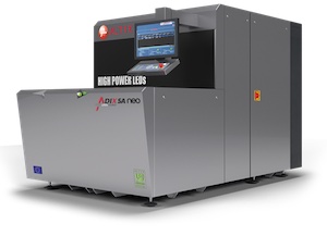
Altix is delighted to announce that the CEA-Liten has ordered an Adix SA for fine line applications to be part of the their research activities focused on micro and nano-technologies, smart digital systems and renewable energy.
With their latest DI imaging down to less than 10µm, the Liten branch will be able to take structural electronics prototyping to the next step. This new Adix will be installed inside Liten’s latest generation clean room dedicated to the research & prototyping of new technologies in the sphere of energy and materials.
Frédéric Baradel, Altix VP, confides: “Bringing our Direct Imaging solution to the CEA is a major milestone as we keep pushing our machine specifications for fine-line applications further. Our sub-10µm-capable installed based is growing steadily and will continue to in the years to come.
About Altix
Altix, a French company located in Val-De-Reuil, Normandy, has been manufacturing cutting edge exposure units since 1991. With more than 600 machines in service worldwide, the company is ??establishing itself as a leader in image transfer machinery around the globe. Altix has subsidiaries in China and North America to ensure reliable and efficient customer support on all continents. For more information, visit www.altix.fr/en/.
Suggested Items
I-Connect007’s Editor’s Choice: Five Must-Reads for the Week
07/04/2025 | Marcy LaRont, I-Connect007For our industry, we have seen several bullish market announcements over the past few weeks, including one this week by IDC on the massive growth in the global server market. We’re also closely watching global trade and nearshoring. One good example of successful nearshoring is Rehm Thermal Systems, which celebrates its 10th anniversary in Mexico and the official opening of its new building in Guadalajara.
Driving Innovation: Direct Imaging vs. Conventional Exposure
07/01/2025 | Simon Khesin -- Column: Driving InnovationMy first camera used Kodak film. I even experimented with developing photos in the bathroom, though I usually dropped the film off at a Kodak center and received the prints two weeks later, only to discover that some images were out of focus or poorly framed. Today, every smartphone contains a high-quality camera capable of producing stunning images instantly.
United Electronics Corporation Advances Manufacturing Capabilities with Schmoll MDI-ST Imaging Equipment
06/24/2025 | United Electronics CorporationUnited Electronics Corporation has successfully installed the advanced Schmoll MDI-ST (XL) imaging equipment at their advanced printed circuit board facility. This significant technology investment represents a continued commitment to delivering superior products and maintaining their position as an industry leader in precision PCB manufacturing.
Orbel Corporation Integrates Schmoll Direct Imaging
06/04/2025 | Schmoll AmericaOrbel Corporation in Easton, PA, proudly becomes the first PCM facility in the U.S. equipped with Schmoll’s MDI Direct Imaging system. This installation empowers Orbel to support customers with greater precision and quality.
Key Insights on Photoresist for Defect Reduction
05/21/2025 | I-Connect007 Editorial TeamIn PCB manufacturing, understanding the intricacies of the photoresist process is crucial for achieving high-quality results. Industry experts Josh Krick, a technical service engineer at IEC, and Tim Blair, a PCB imaging specialist at Tim Blair LLC, share their knowledge on the essential stages of photoresist application, highlight critical advancements in materials, and discuss common defects encountered during production. They share best practices and innovative solutions to enhance the manufacturing process, reduce defects, and ensure efficiency and reliability in high-tech applications.