


 Dan’s Biz Bookshelf: ‘The Next RenAIssance: AI and the Expansion of Human Potential’
 The Chemical Connection: When the Industry Moves Faster Than the Standards
 Driving Innovation: Selecting the Right Laser Source


Rogers Increasing Capacity to Meet Growing Demands for Power Module Substrates
February 16, 2022 | Rogers CorporationEstimated reading time: 1 minute
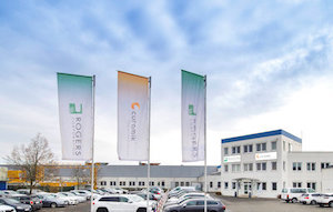
Rogers Corporation’s Advanced Electronics Solutions (AES) announced a further multi-million Euro investment into its site in Eschenbach, Germany, to add to the expansion plans first announced in August 2021. This additional investment will increase capacity of curamik® AMB (Active Metal Brazed) and DBC (Direct Bonded Copper) substrates and allow Rogers to meet the growing demand in the automotive, renewable energy and industrial market segments. The first phase of the expansion is slated for completion in the second half of 2022, with ongoing increases coming on line throughout 2023.
“This investment is a clear demonstration of our commitment to meet the increasing performance and volume requirements of our global customers”, said Roger Tushingham – VP and GM of curamik®. “For many years our teams have done an exceptional job of providing our customers with innovative power substrate solutions that they can rely on. This expansion in capacity will help us meet the expectations of our loyal existing customers, in addition to allowing us to service the ever-expanding customer base in the markets that we serve.”
This is the latest in a series of investments totaling tens of millions of Euro in the production capacity and capability at the Eschenbach location. Whereas earlier investments have been focused on advanced AMB capability, this current investment round will increase the capability and capacity across the entire curamik portfolio.
Share on:


Testimonial
"The I-Connect007 team is outstanding—kind, responsive, and a true marketing partner. Their design team created fresh, eye-catching ads, and their editorial support polished our content to let our brand shine. Thank you all! "
Sweeney Ng - CEE PCBSuggested Items
Driving Innovation: Selecting the Right Laser Source
04/28/2026 | Simon Khesin -- Column: Driving InnovationWhen I first joined Schmoll Maschinen, I brought experience from almost every PCB process, except for laser. As I immersed myself in laser processing, I realized why it can seem so daunting to a newcomer. The complexity arises from three intersecting factors: A vast variety of laser sources: CO2, UV-nano, green-pico, UV-pico, IR-pico, and others; a diverse range of applications: Drilling, cutting, ablation, and more; and an extensive list of materials: These have vastly different absorption rates. Choosing the right machine or laser source is rarely trivial. Even for experienced engineers, answering "Which source is best?" requires examining the business's specific goals.
Institute of Circuit Technology Spring Seminar 2026: A Bright Future in Europe
04/23/2026 | Pete Starkey, I-Connect007Through the leafy lanes and spring flowers of Warwickshire and back to Meridan, the traditional centre of England, and now officially part of the Metropolitan Borough of Solihull in the county of the West Midlands, I attended the Annual General Meeting and Spring Seminar of the Institute of Circuit Technology (ICT) on April 14. Out of the AGM came notable changes in leadership at the top of the Institute: the retirement of Mat Beadel as chair and Emma Hudson as technical director. Effective May 1, Steve Driver is the new chair, and Alun Morgan is the new technical director.
ACCM Unveils Negative and Near-zero CTE Materials for Large-Format AI Chips
04/21/2026 | Advanced Chip and Circuit MaterialsAdvanced Chip and Circuit Materials, Inc. (ACCM) has launched two new materials: Celeritas HM50, with a negative coefficient of thermal expansion (CTE) of -8 ppm/°C to offset the positive CTE and expansion of copper with temperature on circuit boards, and Celeritas HM001, with near-zero CTE and the low-loss performance needed for high-speed signal layers to 224 Gb/s and faster in artificial intelligence (AI) circuits.
Fresh PCB Concepts: Designing PCBs for Harsh Environments—Reliability Is Engineered Upstream
04/23/2026 | Team NCAB -- Column: Fresh PCB ConceptsWhen engineers hear the phrase “harsh environment,” they usually think of the extreme temperature swings, vibration and shock, pressure changes, or radiation in aerospace. However, aerospace is not the only harsh environment where electronic assemblies must survive. Automotive power electronics, downhole oil and gas tools, marine controls, rail systems, defense platforms, and industrial automation equipment all expose PCBs to environments that are equally unforgiving. The stress mechanisms may differ, but the physics does not.
Advanced Packaging for AI: Reliability Starts at the Cu/Cu/Cu Microvia Junction
04/20/2026 | Kuldip Johal, MKS' AtotechThe rapid growth of AI computing, from training clusters to inference at scale, is reshaping demand across the entire electronics supply chain. Advances in technology requirements, such as higher bandwidth, lower latency, and greater compute density, are driving the development of advanced packaging technologies and transforming the PCB industry across design, manufacturing, testing, and even architecture.