


 Dan’s Biz Bookshelf: ‘The Next RenAIssance: AI and the Expansion of Human Potential’
 The Chemical Connection: When the Industry Moves Faster Than the Standards
 Driving Innovation: Selecting the Right Laser Source


MacDermid Alpha to Exhibit, Present at the IMAPS Device Packaging Conference
February 17, 2022 | MacDermid Alpha Electronics SolutionsEstimated reading time: 1 minute
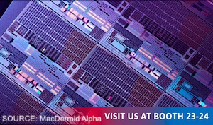
MacDermid Alpha Electronics Solutions, a global supplier of integrated solutions from our Circuitry, Assembly and Semiconductor divisions that provides unmatched capabilities in electronics design and manufacturing, will be exhibiting and presenting a paper at the IMAPS Device Packaging Conference at the WeKoPa Resort and Conference Center, Fountain Hills, AZ, March 7-10, 2022.
Jianwen Han, Principal Research Scientist, will be presenting “Electrochemical Plating System Development of Nano-twinned Cu for Multiple WLP Features”. The paper discusses the development of a series of electrochemical plating baths and processes, generating nano-twinned Cu in wafer-level packaging applications to fulfill the expanding market demand for copper-to-copper direct bonding and hybrid-bonding. This newly developed system shows a high density of nt-Cu (close to 100%), controllable grain size (0.10 to 1.0 micron), vertical columnar structure, and minimal transition layer between Cu seed and nt-Cu initial position.
Featured in the booth will be the MacDermid Enthone brand of product offerings from the Circuitry Solutions division that enable upgraded FCCSP and PCBGA fabrication. Highlighted will be the entire Systek family of high-performance build-up processes for IC Substrates and their integrated leadframe product portfolio which incorporates connected solutions and spans the entire process of building QFN packages from leadframe roughening to enhancing sidewall solderability for enhanced reliability.
The Alpha, Kester, and MacDermid Enthone brands from the Semiconductor division will promote MICROFAB EVF NiBAR, a boric acid free sulfamate nickel electroplating process for semiconductor applications and ATROX CF200-1D an electrically conductive die attach film with thermal conductivity of >20 W/m-K. Also highlighted will be their complete line of STAYSTICK and STAYCHIP adhesives for structural and functional bonding.
The Compugraphics brand, will showcase their complete line of photomask solutions and support services. From 1X master photomasks and reticles to pellicle replacement, MPT coating and photomask cleaning, with quick-turn service, they are a partner you can reply on.
MacDermid Alpha’s team of industry experts from their Circuitry and Semiconductor divisions will be available at booth #23/24 to discuss the challenges the semiconductor and IC substrate manufacturing sectors face as technology continues to push the limits of performance and miniaturization.
Share on:


Testimonial
"Advertising in PCB007 Magazine has been a great way to showcase our bare board testers to the right audience. The I-Connect007 team makes the process smooth and professional. We’re proud to be featured in such a trusted publication."
Klaus Koziol - atgSuggested Items
Driving Innovation: Selecting the Right Laser Source
04/28/2026 | Simon Khesin -- Column: Driving InnovationWhen I first joined Schmoll Maschinen, I brought experience from almost every PCB process, except for laser. As I immersed myself in laser processing, I realized why it can seem so daunting to a newcomer. The complexity arises from three intersecting factors: A vast variety of laser sources: CO2, UV-nano, green-pico, UV-pico, IR-pico, and others; a diverse range of applications: Drilling, cutting, ablation, and more; and an extensive list of materials: These have vastly different absorption rates. Choosing the right machine or laser source is rarely trivial. Even for experienced engineers, answering "Which source is best?" requires examining the business's specific goals.
Institute of Circuit Technology Spring Seminar 2026: A Bright Future in Europe
04/23/2026 | Pete Starkey, I-Connect007Through the leafy lanes and spring flowers of Warwickshire and back to Meridan, the traditional centre of England, and now officially part of the Metropolitan Borough of Solihull in the county of the West Midlands, I attended the Annual General Meeting and Spring Seminar of the Institute of Circuit Technology (ICT) on April 14. Out of the AGM came notable changes in leadership at the top of the Institute: the retirement of Mat Beadel as chair and Emma Hudson as technical director. Effective May 1, Steve Driver is the new chair, and Alun Morgan is the new technical director.
ACCM Unveils Negative and Near-zero CTE Materials for Large-Format AI Chips
04/21/2026 | Advanced Chip and Circuit MaterialsAdvanced Chip and Circuit Materials, Inc. (ACCM) has launched two new materials: Celeritas HM50, with a negative coefficient of thermal expansion (CTE) of -8 ppm/°C to offset the positive CTE and expansion of copper with temperature on circuit boards, and Celeritas HM001, with near-zero CTE and the low-loss performance needed for high-speed signal layers to 224 Gb/s and faster in artificial intelligence (AI) circuits.
Fresh PCB Concepts: Designing PCBs for Harsh Environments—Reliability Is Engineered Upstream
04/23/2026 | Team NCAB -- Column: Fresh PCB ConceptsWhen engineers hear the phrase “harsh environment,” they usually think of the extreme temperature swings, vibration and shock, pressure changes, or radiation in aerospace. However, aerospace is not the only harsh environment where electronic assemblies must survive. Automotive power electronics, downhole oil and gas tools, marine controls, rail systems, defense platforms, and industrial automation equipment all expose PCBs to environments that are equally unforgiving. The stress mechanisms may differ, but the physics does not.
Advanced Packaging for AI: Reliability Starts at the Cu/Cu/Cu Microvia Junction
04/20/2026 | Kuldip Johal, MKS' AtotechThe rapid growth of AI computing, from training clusters to inference at scale, is reshaping demand across the entire electronics supply chain. Advances in technology requirements, such as higher bandwidth, lower latency, and greater compute density, are driving the development of advanced packaging technologies and transforming the PCB industry across design, manufacturing, testing, and even architecture.