


 Beyond the Board: What Companies Need to Know Before Entering the MilAero PCB Market
 Defense Speak Interpreted: If CHIPS Cuts Back, What Happens to Electronics Packaging Funds?
 American Made Advocacy: Where’s the Budget for a Modern Military Run on Microelectronics?


Teledyne Labtech Announces New Advanced Graphite Embedding Capability for PCB Thermal Management
March 16, 2022 | Business WireEstimated reading time: 1 minute
Teledyne Labtech announces a major new capability allowing the embedding of layers of synthetic graphite within RF and microwave printed circuit boards (PCBs). Heat management is a significant concern in many aerospace, defense and space applications where size, weight and power (SWaP) are key attributes. Gallium nitride (GaN) solid state power amplifiers (SSPAs) are examples of increasingly common devices that benefit from careful heat management. This new technique allows efficient conduction of heat away from such devices, saving system weight and increasing their lifetime.
Managing waste heat is a significant problem in today’s electronic systems, impacting reliability and requiring added expense and weight to control effectively. In the latest consumer mobile phones, it is common to employ sheets of self-adhesive synthetic graphite on top of critical semiconductor devices in order to conduct away waste heat from small areas. Aerospace, defense and space applications require more precision, repeatability and area of coverage. To address this, Teledyne Labtech has developed a method of embedding thin layers of synthetic graphite inside the structure of the host PCB reliably, saving size and weight, while increasing the lifetime of active devices (MTBF) by permitting operation at cooler steady state.
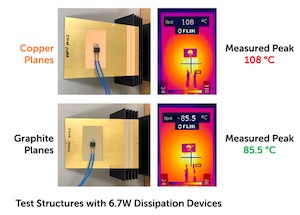
“Synthetic graphite is 4 times lighter than copper, and transfers heat 4 times better in the X-Y plane,” said John Priday, CTO of Teledyne Labtech. “Replacing PCB ground plane layers with it in critical applications such as T/R modules can cause devices to run up to 20°C cooler in our testing.”
Labtech has demonstrated that thermal copper layers can be replaced with the new graphite technique while remaining reliable and experiencing minimal impact on the passage of microwave signals on grounding layers.
Share on:


Testimonial
"Our marketing partnership with I-Connect007 is already delivering. Just a day after our press release went live, we received a direct inquiry about our updated products!"
Rachael Temple - AlltematedSuggested Items
Electrodeposited Copper Foils Market to Grow by $11.7 Billion Over 2025-2032
09/18/2025 | Globe NewswireThe global electrodeposited copper foils market is poised for dynamic growth, driven by the rising adoption in advanced electronics and renewable energy storage solutions.
MacDermid Alpha Showcases Advanced Interconnect Solutions at PCIM Asia 2025
09/18/2025 | MacDermid Alpha Electronics SolutionsMacDermid Alpha Electronic Solutions, a global leader in materials for power electronics and semiconductor assembly, will showcase its latest interconnect innovations in electronic interconnect materials at PCIM Asia 2025, held from September 24 to 26 at the Shanghai New International Expo Centre, Booth N5-E30
Trouble in Your Tank: Implementing Direct Metallization in Advanced Substrate Packaging
09/15/2025 | Michael Carano -- Column: Trouble in Your TankDirect metallization systems based on conductive graphite are gaining popularity throughout the world. The environmental and productivity gains achievable with this process are outstanding. Direct metallization reduces the costs of compliance, waste treatment, and legal issues related to chemical exposure. A graphite-based direct plate system has been devised to address these needs.
Closing the Loop on PCB Etching Waste
09/09/2025 | Shawn Stone, IECAs the PCB industry continues its push toward greener, more cost-efficient operations, Sigma Engineering’s Mecer System offers a comprehensive solution to two of the industry’s most persistent pain points: etchant consumption and rinse water waste. Designed as a modular, fully automated platform, the Mecer System regenerates spent copper etchants—both alkaline and acidic—and simultaneously recycles rinse water, transforming a traditionally linear chemical process into a closed-loop system.
Driving Innovation: Depth Routing Processes—Achieving Unparalleled Precision in Complex PCBs
09/08/2025 | Kurt Palmer -- Column: Driving InnovationIn PCB manufacturing, the demand for increasingly complex and miniaturized designs continually pushes the boundaries of traditional fabrication methods, including depth routing. Success in these applications demands not only on robust machinery but also sophisticated control functions. PCB manufacturers rely on advanced machine features and process methodologies to meet their precise depth routing goals. Here, I’ll explore some crucial functions that empower manufacturers to master complex depth routing challenges.