


 It’s Only Common Sense: Stay Curious, My Friends
 The Marketing Minute: AI Is Watching Your Marketing Habits
 Trouble in Your Tank: The Role of Organic Solderability Preservatives in Advanced Packaging
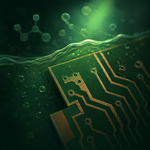


We recently spoke with Dave Torp, CEO of Winonics, about the company’s additive and semi-additive processes and what PCB designers need to know if they’re considering designing boards with these new technologies. As Dave explains, additive design is not much different from traditional design, but the steps in the design cycle are out of order, and additive designers must communicate with their fabricators because so much of the new processes are still proprietary.
Andy Shaughnessy: Dave, give us some background on Winonics and your focus on additive and semi-additive processes.
Dave Torp: Additive Circuits Technologies is the parent company, which owns two companies. One is Winonics, a rigid circuit board company. The other is a flexible circuit board company called Bench 2 Bench. Winonics is ISO-9001, AS 9100, and ITAR-registered. We have a 52,000 square-foot facility in Brea, California. Bench 2 Bench has a 25,000 square-foot facility, located about 10 minutes away in Fullerton.
From the holistic view, our focus is in the high-reliability electronics market. We focus on the aerospace, defense, and the medical device electronics. Our competitive anchor is providing great service. We don’t really put too many boundaries on what we do. Simply put, we’re a technology realization company.
We have process patents for applying circuitry and metallization in an additive technology. We also have some trade secrets that we keep behind the vest with respect to our manufacturing operations. What the additive technology enables is ultra-fine features and ultra-high definition. The enabling technology provides metallization in very high-density configurations to make high-density interconnects. We have demonstrated the technology down to 15-micron lines and spaces, which was, at the time, the limit of the laser technology that we had.
As the LDI technology becomes more precise, we’ll have the ability to go further down that pathway. So, we look to being capable of doing 8-micron lines and spaces and below by 2023.
The real drivers for the technology are miniaturization and the need for greater speed. If you look at some of the frequencies that are required to enable a communication, you are getting up into the 5G-plus mindset. The layer counts within the circuit boards aren’t increasing, but the number of interconnects between those layers is increasing. You can have a lot of fun with respect to the layers that are being interconnected and how the microvias are being stacked and racked upon each other. Sometimes you stack them right on top of each other. Other times, you stagger them out a little bit, depending on the signal integrity that you want.
With respect to the additive processes, first we have semi-additive technology, which is a fairly new process. In a lot of cases, you take the ultra-thin copper foils, or the plating applied to the substrate. You hit it with photo-sensitive materials, etch away that ultra-thin part of the copper, and then start to plate back up. That’s the semi-additive process.
The fully additive process is the newest technology, where you print the pattern that you want on the substrate without copper foil, using a palladium or platinum-based chemistry, and expose it with a laser or a UV source of radiation. Then you allow the electroless copper plating to be deposited, followed by electrolytic plating
This allows us to create ultra-fine traces down to sub-15-micron type technology. We’re excited about the opportunities, especially in the in-betweens, where you’re using hybrid interposer layers to try to connect this heterogeneous integrated package together.
To read this entire conversation, which appeared in the April 2022 issue of Design007 Magazine, click here.


