


 The Marketing Minute: Marketing With Layers
 The Right Approach: Electro-Tek—A Williams Family Legacy, Part 1
 It’s Only Common Sense: If You’re Not Differentiated, You’re Dead


Altus Respond to Koh Young’s Successful New Semicon Focused Inspection System
May 18, 2022 | Altus GroupEstimated reading time: 1 minute
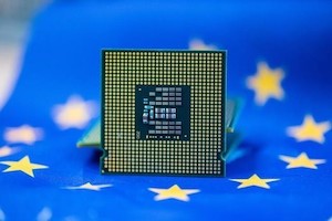
Returning from supporting their pre-eminent suppliers at SMTconnect in Germany, Altus Group, a leading distributor of capital equipment in the UK and Ireland, has reported an increased interest in many products including Koh Young’s new Meister S High-Resolution Inspection system.
Launched at the SMTconnect, which welcomed industry leaders from the global electronics community, Meister Model S was central on Koh Young’s stand and drew much attention from visitors at the show.
Building on the popular range of inspection platforms in both AOI and SPI processes, the Meister is the industry’s leading inspection system for advanced packaging and semiconductors. The new Meister S model includes a 3.5 µm pixel resolution and a 25 MP high-speed camera.
Anthony Oh, Technical Applications Manager, Altus said: “The reaction to the new Meister S at SMTconnect, and since returning from the show, has been extremely positive. The new S Model was developed to meet the demand for Wafer-Level-Packaging applications.
“Koh Young reported that the average bump size of 70 µm will decrease to 50 µm in the near future. To meet the impending demand, Meister S was developed with a new camera optimized for high-speed image acquisition in a 24/7 production environment. The system also includes an updated lens system. It is an impressive addition to the AOI line-up and we predict it will be a popular choice for our customers this year.
“Any addition to Koh Young’s equipment portfolio is very welcome by the Altus team. As a world-class leader in 3D measurement-based inspection solutions, we know that their new system will be of the highest quality and a sound investment for our customers.”
Additional content from Koh Young:
- The Printed Circuit Assembler’s Guide to… SMT Inspection: Today, Tomorrow, and Beyond by Brent Fischthal
- “Converting Process Data Into Intelligence” by Joel Scutchfield and Ivan Aduna, a free 12-part micro webinar series
- You can also view other titles in our full I-007e book library here
Share on:


Testimonial
"Your magazines are a great platform for people to exchange knowledge. Thank you for the work that you do."
Simon Khesin - Schmoll MaschinenSuggested Items
Light-curable Solutions for Reliable Electronics in Space Applications
10/15/2025 | Virginia Hogan, DymaxDesigning electronics for space environments, particularly those in low Earth orbit (LEO), requires careful consideration of materials that can withstand extreme conditions while supporting long-term reliability. Engineers designing satellite systems, aerospace instrumentation, and high-altitude platforms face a familiar set of challenges: contamination control, mechanical stress, thermal cycling, and manufacturability.
Analog Devices Launches ADI Power Studio™ and New Web-Based Tools
10/14/2025 | Analog Devices, Inc.Analog Devices, Inc., a global semiconductor leader, announced the launch of ADI Power Studio, a comprehensive family of products that offers advanced modeling, component recommendations and efficiency analysis with simulation. In addition, ADI is introducing early versions of two new web-based tools with a modernized user experience under the Power Studio umbrella:
Elementary, Mr. Watson: High Power: When Physics Becomes Real
10/15/2025 | John Watson -- Column: Elementary, Mr. WatsonHave you ever noticed how high-speed design and signal integrity classes are always packed to standing room only, but just down the hall, the session on power electronics has plenty of empty chairs? It's not just a coincidence; it's a trend I've observed over the years as both an attendee and instructor.
Beyond Thermal Conductivity: Exploring Polymer-based TIM Strategies for High-power-density Electronics
10/13/2025 | Padmanabha Shakthivelu and Nico Bruijnis, MacDermid Alpha Electronics SolutionsAs power density and thermal loads continue to increase, effective thermal management becomes increasingly important. Rapid and efficient heat transfer from power semiconductor chip packages is essential for achieving optimal performance and ensuring long-term reliability of temperature-sensitive components. This is particularly crucial in power systems that support advanced applications such as green energy generation, electric vehicles, aerospace, and defense, along with high-speed computing for data centers and artificial intelligence (AI).
Bluepath Robotics Optimizes AMR Fleets with Inductive Charging Solution from Wiferion
10/09/2025 | WiferionIn a dynamic and highly competitive industry such as logistics, efficient and uninterrupted material flows are of crucial importance. To ensure maximum uptime for its robots, Bluepath Robotics, which specializes in autonomous mobile robots (AMR), needed a reliable and powerful power supply.